- Forums
- Product Forums
- General Purpose MicrocontrollersGeneral Purpose Microcontrollers
- i.MX Forumsi.MX Forums
- QorIQ Processing PlatformsQorIQ Processing Platforms
- Identification and SecurityIdentification and Security
- Power ManagementPower Management
- Wireless ConnectivityWireless Connectivity
- RFID / NFCRFID / NFC
- MCX Microcontrollers
- S32G
- S32K
- S32V
- MPC5xxx
- Other NXP Products
- S12 / MagniV Microcontrollers
- Powertrain and Electrification Analog Drivers
- Sensors
- Vybrid Processors
- Digital Signal Controllers
- 8-bit Microcontrollers
- ColdFire/68K Microcontrollers and Processors
- PowerQUICC Processors
- OSBDM and TBDML
- S32M
-
- Solution Forums
- Software Forums
- MCUXpresso Software and ToolsMCUXpresso Software and Tools
- CodeWarriorCodeWarrior
- MQX Software SolutionsMQX Software Solutions
- Model-Based Design Toolbox (MBDT)Model-Based Design Toolbox (MBDT)
- FreeMASTER
- eIQ Machine Learning Software
- Embedded Software and Tools Clinic
- S32 SDK
- S32 Design Studio
- GUI Guider
- Zephyr Project
- Voice Technology
- Application Software Packs
- Secure Provisioning SDK (SPSDK)
- Processor Expert Software
-
- Topics
- Mobile Robotics - Drones and RoversMobile Robotics - Drones and Rovers
- NXP Training ContentNXP Training Content
- University ProgramsUniversity Programs
- Rapid IoT
- NXP Designs
- SafeAssure-Community
- OSS Security & Maintenance
- Using Our Community
-
- Cloud Lab Forums
-
- Knowledge Bases
- ARM Microcontrollers
- i.MX Processors
- Identification and Security
- Model-Based Design Toolbox (MBDT)
- QorIQ Processing Platforms
- S32 Automotive Processing Platform
- Wireless Connectivity
- CodeWarrior
- MCUXpresso Suite of Software and Tools
- MQX Software Solutions
- RFID / NFC
-
- Home
- :
- i.MX论坛
- :
- i.MX RT 交叉 MCU
- :
- Re: Large current surge problem during power sequencing of i.MX RT 1052 Rev. A
Large current surge problem during power sequencing of i.MX RT 1052 Rev. A
Large current surge problem during power sequencing of i.MX RT 1052 Rev. A
Hi All
We are having problems bringing up the boards with i.MX RT 1052A parts due to the fact that when the power sequencing is performed (to work around the errata) there is often a large surge of current which causes the power supply to cut out and thus the sequence to restart. Sometimes it manages to start but sometimes it fails to ever start.
During the investigation to date I have made various recordings showing the voltages and there is one clear indication of whether it will fail or not so I will describe in some detail in the hope that this can be explained and something can be adjusted to be able to power the processor up reliably.
1. We use an KL02 in order to be able to accurately power sequence the supply rails and also to allow various modes to be set based on a single push button input (eg. reset of processor, power cycle of processor, force to ISP mode without needing DIP switches). This means that I have the possibility to change the sequencing details and timing and in the following I have slowed it down somewhat so that the steps are more evident (about 100ms between steps, instead of just a few ms that would normally be required).
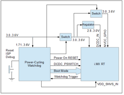
2. The KL02 can disable/enable the main 3V3 to the processor. It controls its DCDCSWITCH input, its POR and also controls a second switch of the main power to the GPIO rail. Its block diagram is shown here:
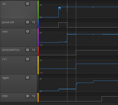
2. Here is a typical power up sequence that operates 'normally' when the main power is applied (100ms unit shown)
Vin is the main 3V3 power supply on the board that is also supplying the KL02. Initially there is no voltage applied to the i.MX RT 1052A.
(slowed down sequence)
- After 100ms (to ensure all is stable) the KL02 switches the 3V3 to the processor (but not yet GPIO 3V3) (power ctrl goes low and vout is applied)
- 100ms later the KL02 sets the DCDCSWITCH input to '1' so that the on-chip 1V1 DC/DC converter starts (takes about 1..2ms to output accurate 1.1V)
- 100ms later the KL02 applies VDD_SNVS (but not visible in this recording and unlikely to be relevant)
- 100ms later the KL02 enables the second switch to connect 3V3 to the GPIO rails, which, according to the errata, should not be applied before the other voltages are all present.
- Finally, after another 100ms, the KL02 sets the POR high so that the i.MX RT 1052A can actually start.
The first observation is that the GPIO 3V3, although not switched through, rises as the different steps are performed.
Immediately it rises to 0.7V although no power is applied - presumably due to a leakage path somewhere.
Then it rises again (RC curve taking about 20ms) once the 1v1 voltage (internal DC/DC converter) is operating (to about 2.7V so presumably leakage path from the DCDC input or VDD_HIGH_IN (connected to DCDC_IN) or even VDDA_ADC_3P3 (also connected to DCDC_IN).
When the GPIO rail switch is enabled it then rises to 3.3V and all power is applied.
I note that there are (small) input current surges when the main power is switched through, the DC/DC is enabled and when the GPIO 3V3 is switch through (small glitches visible on VIN) but these are not sources of disturbance in this case.
I have removed all other circuitry on the GPIO 3V3 to ensure that this can't originate from something else sharing the power rail.
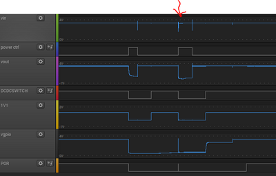
3. The next sequence shows a consistent behavior which is seems to characterise the main issue. The KL02 can control a power cycle and this shows it taking place.
Initially the KL02 sets the POR low (to set the processor to reset state) and then disables all power switches and DCDC converter. As can be seen the 1V1 falls to 0V. GPIO 3V3 falls to about 0.4V and Vout falls to about 0.7V. After 65ms it performs the power cycling sequence again.
The difference is however that GPIO 3V3 doesn't rise to 0.7V when the DCDC_IN is applied. Also it stays about the same when the DCDC convert is enabled.
At the point when the GPIO 3V3 is switched (red arrow) there is a large glitch on the main power supply (I have measured up to 1A of surge current) which causes the KL02 itself to reset.
The KL02 then performs the same start up sequences after its power up and in this case it works and it is seen that also the GPIO 3V3 rail then follows the step form that was originally seen rather then being in what looks like a 'clamped' state.
Therefore the startup is mostly Ok and the power cycle works, but it only works on the second attempt (with the complete power supply collapsing at one point due to a high current - it falls to < 1.5V and triggers the KL02's brown out reset).
4. Unfortunately sometimes the board never starts - this happens mostly when it has been powered down for a few seconds - when powered down for a longer period it is much less likely.
In such cases it does the following:
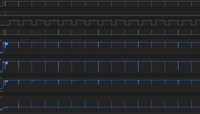
Here it attempts to start but the GPIO 3V3 is always at 0.7V and as soon as the GPIO 3V3 switch is enabled the current surge cause the power supply to collapse and it restarts and repeats. Sometimes it may start after some time abut essentially it is stuck in this loop (here it tries every 300ms).
All voltages generate by the i.MX RT 1052 itself are accurate.
I believe we have respected accurately all workarounds but obviously the power-up issue is serious and requires a very strong and stable source capable of driving 1A in order to be able to start, after which the idle consumption from 3V3 is about 15mA.
Is it possible to explain what is being seen and whether it is related to the chip's erratas? How can we work around it?
Thanks in advance.
Regards
Mark
Hi Mark
1. ERR011092 says "Apply power to DCDC_IN/DCDC_IN_Q with DCDC_PSWITCH pin, 1ms ahead of
VDD_SNVS_IN" - have you tried doing exactly that?
2. What is powering the 3V3, presumably a point-of-load regulator somewhere? What is the transient response of the chosen device? Can you try powering using a different device or even from a bench PSU?
3. How is the PCB layout? Adequate decoupling located close by? Low inductance?
4. Have you/can you try A1 silicon?
5. What happens if you effectively remove the KL02 and the power switches etc.... from the system, and power the chip "normally" without all the external controls (but just delaying SNVS to respect the errata)?
-Nick
Hi Nick
1. There are three erratas (in all, 4 points) to be worked around and the SNVS IN one is not that critical but initially I had all timing according to the recommendation but slowed it down to better see what happens at each step - overall it doesn't change anything.
2. 3V3 is from a 1A DC/DC converter but I also power from a lab supply for comparisons - I need to set over 1A current limit at the supply for it to survive the GPIO switch and therefore it is the high current that is the main issue at that moment in time. The DC/DC converter's transient response may not be ideal but at the moment it is not the limiting factor and whether it is relevant or not depends on the load switching and if it is possible to work around these current spikes the DC/DC converter behavior itself becomes less relevant.
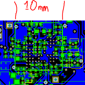
3. Layout follows the guide with all decoupling under the chip with very short paths and the (large) number of decoupling caps:
4. We had to purchase a large quantity of available A parts (which presumably no one else wanted to touch) since the B parts are not deliverable at the moment. I believe a very small quantity of B parts have been found in the meantime but, due to the BGA, it would not be possible to quickly experiment. I have the 1050 EVK with B part for comparison but that is difficult to modify and I don't know whether it will help much apart from possibly proving that newer parts are better. It won't help the fact that we need to deliver thousands of boards with the available A parts as soon as possible.
5. The most critical workaround is to not apply the GPIO power rail before the rest is stable since if all is applied together there is an inrush current that can damage the chip and this is why I am reluctant to remove the delay but I may do it on one board as reference. If I am in fact (sometimes) still seeing this high inrush current even when the workaround have been applied it means the described workaround is not adequate on its own. maybe I need to actively discharge any voltage on the rail before switching, or something like that???
Regards
Mark
Hi All
After several days of attempting to get the boards to come up and work there has not yet been any progress and the work-arounds are temporarily being abandoned in an attempt to bring up the processor even if there is a risk of the DC/DC converter not starting or damage due to GPIO surges (although the GPIO power connection is mainly interrupted to reduce/remove this risk during most of the testing).
This allows easier direct comparisons with various reference boards with A parts that operate.
At the moment there is only one difference that is visible and that is the behavior of the PMIC_ON_REQ output.
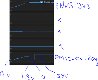
This is how it tends to react (eg. on an 1062B part):
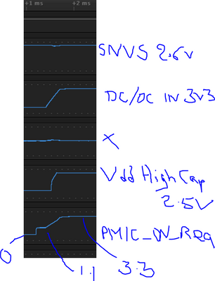
The 1052A board in question:
It is seen that (other voltages not displayed since DCDC switching is delayed longr) rather than staying at 0V from SNVS IN being applied it already ramps up before then falling to 0V. After about 2ms (similar to the reference) it then rises directly to 3.2V, whereby the reference switched the output initially to 1.1V.
Does this give any clues?
Regards
Mark
Hi Mark,
As you may know already, the RT105A is the first version of the silicon. Several bugs have been fixed in the newer silicon version. Considering the nature of the issue and the erratas that have been addressed in the A1 silicon, the support will be limited. I understand that due to the current situation you decided to use this version of the chip. I will check this matter internally with the applications team, however, I do not want to give you any false expectations.
Regards,
Victor
Hi Victor
We had a meeting with NXP a few weeks ago where the strategy to use the A parts before migrating to the B parts was discussed and approved.
The case is being handled by a direct contact but there is also the same problem that it is being blocked to a degree due to the depreciated parts, but we are still hoping that via one of the channels there may be some insider knowledge that can be exchanged that may allow the main issue(s) to be identified/understood/resolved.
At this moment in time we have what looks like a reliable power up of the processor (all voltages are available with their expected accuracy) but using more powerful supplies which are still requiring several fast attempts to start - but look to achieve it within about 40ms at the most.
The issue that is still blocking (the most) is that it is not possible to program the boards - this is discussed here: https://community.nxp.com/t5/i-MX-RT/No-USB-ISP-Operation-on-i-MX-RT-1052A/m-p/1325836#M15937
It may well be that the power supply is the root cause but we know that the processor is trying to boot (QSPI access at the extended 33MHz) and the boot loader is presumably in the ISP mode due to the fact that the HS USB low level is working perfectly (must have been correctly initialised by the boot loader) but the i.MX RT 1052 is only ever returning NAKs when the initial device descriptor is received.
SWD is not communicating at all.
Power consumption when POR is low is about 20mA and when POR is high and the HS USB operating it is about 80mA.
We may be able to try with a 1062 B part in a few days to see what the differences are bit we absolutely need to be able to deliver a large quantity with 1052 A in order to be able fulfill contracts and then move to the new silicon (when it can be delivered).
Regards
Mark
Thanks for the response, Mark. I'm reviewing this case with the distributor as well. At this point, there's a lot of information from your end and the distributor's end. Due to this, I would like to confirm that we are on the same page. The problem that you are facing is during the power-up sequence, correct? Based on the tests you have made seems that the problem comes from NVCC_GPIO since this voltage rises to 0.7 when you power on other voltages, correct?
Regards,
Victor
Hi Victor
Presently we have two problems:
1. The power up is not reliable due to large current surges, as explained here.
2. Neither SWD nor ISP is working correctly - see other post, whereby the ISP programming is the main issue (I think I know why the SDW is not working now and it would be normal and not a real problem).
The complication with the power up sequence is that it is not always the same. However the errata workarounds have been implemented as accurately as possible and all recordings confirm this. We have modified the PSU in an attempt to combat it and have something that I believe is operating adequately to move on to actual application work with the first boards (but needs revisiting for production release).
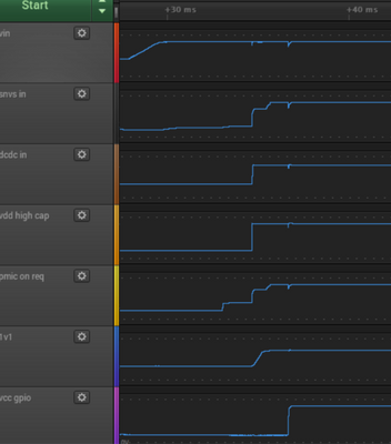
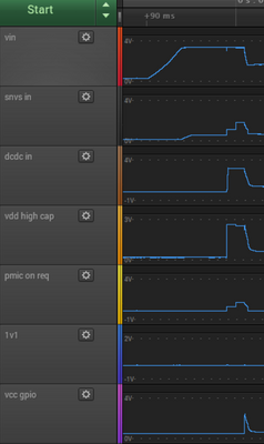
I'll show you a recording where is starts (this is the present state that I believe exactly respects the errata recommendations).
Vin is the main 3V3 input voltage that ramps from 0V to 3.3V.
The KL02 starts and waits 5ms to ensure that this is well charged before continuing since we know that it will be "challenged" later.
DCDCIN (together with VDD_HIGH_IN) is applied at the same time as DCDC_POWER is asserted (not all signals shown) and 1ms later SNVS_IN is applied. DCDC_IN is 2.95V to respect one errata point (VDD_HIGH and SNVS_IN are 3V3) and t is seen that VDD_HIGH_CAP goes to 2.5V (VDD_PLL - not shown - goes to 1.1V).
The VDD_SOC (1.1V) rail ramps up to 1.15V showing the the internal DC/DC converter starts.
VCC_GPIO is switched through 1ms later (errata requires it to be switched 2ms after DCDC_IN).
In this case it charges for about 0.5V to 3.3V, causing some visible glitches but all is OK.
I can't understand the PMIC_ON_REQ form but it is not used (just observation)
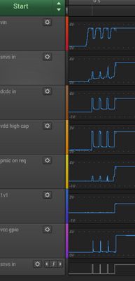
In some other instances it, however, does the following instead:
First of all the 1V1 voltage doesn't appear and then, when GPIO is applied, the input voltage fails when VDD_GPIO is switched through.
At the moment (with the more powerful supply) it tends to fail three times and is successful teh fourth time:
This may be a mixture of the DCDC converter startup errata and the GPIO inrush current errata since, when the VDD_SOC (1V1) is not successful the subsequent GPIO current is huge.
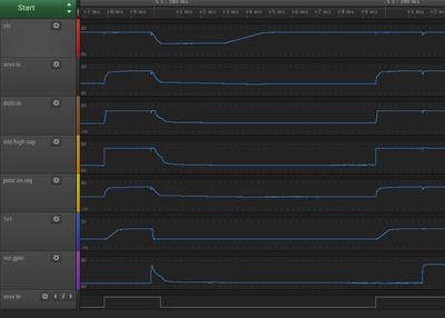
There is however a third situation which tends to take place when the processor is momentarily powered down as show here:
In this case the VDD_SOC (1V1) does come up normally but there is still a high VSDD_GPIO current when it is switched that leads to the input voltage failing. The KL02 restarts and then it is Ok again.
PMIC_ON_REQ and SNVS IN voltages are different in form (influenced presumably be internal chip state).
These also deviate somewhat to other recordings where the timing was slowed down and overall it is not obvious what is contributing to the effects but, although the boards are now starting, it looks like the workaround to ensure the internal DC/DC converter starts is not 100% reliable. When it doesn't start it presumably triggers the next errata with large in-rush current.
More of a nuisance is that the large current can sometimes occur when the internal DCDC convert has started correctly.
Overall we would like to works with the prototypes in this state, hoping that there is no damage being made that will cause further failures.
I could imagine using the KL02's ADC to monitor the DCDC output before switching VDD_GPIO so that it avoids one failure mode and possibly adding a circuit to discharge the GPIO rail before starting to ensure it is not in an some sort of latched state that will cause the same (notice that from the first report there was an intermediate state that failed too).
We know that the i.MX RT 1052 A is a temporary step but we still need to be sure that they will not fail due to random current surges that may be damaging the chip internally.
If there are any observations, information for those who understand what may be taking place internally, and recommendations for improvements these are extremely welcome.
I can adjust timing details and some circuity if needed.
the ISP issue is what we are concentrating on at this moment and hoping that it is not a result of chip damage during power sequencing. All boards are reacting the same with respect to this.
Regards
Mark
Hi Mark,
Thanks for the detailed explanation. Regarding the Serial Downloader problems. My colleague is already working on this in your other thread. Any updates from this topic will go through that thread. As for the power-up sequence, I'm already investigating this internally with the applications team. Due to the revision of the chip you are using, getting a response from the applications team will take longer than usual.
Regards,
Victor
