- 新着としてマーク
- ブックマーク
- 購読
- ミュート
- RSS フィードを購読する
- ハイライト
- 印刷
- 不適切なコンテンツを報告
I want to trigger a 25 byte DMA data transfer on the LPSPI3 being triggered by a dropping edge GPIO input.
I am using: MCUXpresso IDE v11.4.1 [Build 6260] [2021-09-15] toolchain
and working on a IMXRT1060 EVKB development board. (note I did add the needed resistors to support the Arduino pin connections (J17-4, J17-5 & J17-6)
I have mapped the LPSPI3 pins:
* MOSI J23-23
* MISO J23-7
* CLK J23-21
* CS J23-22
I have a signal generator sending a 3.3V square wave pulse to the Arduino pin: J17-6 GPIO_SD_B0_00
(which is configured to use XBAR1_INOUT4)
To confirm that my signal is present I'm mirroring this signal to Arduino pin: J17-5 GPIO_SD_B0_03
(which is configured to use XBAR1_INOUT6)
I have my XBAR output 3 to start DMA channel 8 to set/clear GPIO pin: J17-4 GPIO_SD_B0_02
Channel 8 that is performing the set/clear operations on GPIO_SD_B0_02 is also chained to start the LPSPI3 data transfer, which in turn is changed to a channel 7 to set the GPIO pin.
The sample code can be found and loaded from the following GitHub repo branch develop: https://github.com/tsbiberdorf/SPI3-DMA-FromGPIO.git
The sample code is run by entering a character into the UART port on the EVKB board.
This test can be run by issuing the character '6'. Other tests are made available in this sample code, please read the description if you want to run them, but my concern here is for test '6'.
In this test, I am configured XBAR1 to receive my dropping edge GPIO signal (P17-6). The XBAR1 will then output a DMA operation on XBAR1_INOUT3 to start the DMA0 channel 8.
DMA0-ch8 will clear P17-4 then it should start DMA0-ch6 to execute a 25 byte DMA operation from LPSPI3 peripheral. When this transfer is completed, it will then activate DMA0-ch7 to set pin P17-4.
DMA0-ch5 has been configured to read all data received from LPSPI3 bus. it will also call for a IRQ complete when completed.
DMA0-ch7 will be called to set the Arduino pin P17-4 to signal that the data transfer has been completed.
A major problem that I cannot figure out is why does a part of the SPI3 transfer happen at the start of my test '6', and then when the dma ch8 is completed does it not start again? My guess is that the SPI3 peripheral is locked up, but I'm not sure why or how to fix it.
Can someone please help explain what I am doing wrong?
Thanks
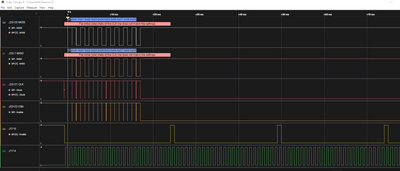
This is what a logic analyzer capture of the listed pins indicates:
so you can see that when command '6' is issued, the XBAR triggers J15-5 to clear and the SPI transfer starts, but does not complete all 25 bytes. it appears that 25 dropping edges of J17-6 is measured (by the mirror on J17-4) till the dma channel 7 is started to set J17-5.
After this first cycle, no further SPI 3 traffic is measured, but the the number of dropping edges does match the number of bytes that should be transferred.
解決済! 解決策の投稿を見る。
- 新着としてマーク
- ブックマーク
- 購読
- ミュート
- RSS フィードを購読する
- ハイライト
- 印刷
- 不適切なコンテンツを報告
I found the solution. I created test case '8', '9', & 'a' to demonstrate the configuration and operations.
- 新着としてマーク
- ブックマーク
- 購読
- ミュート
- RSS フィードを購読する
- ハイライト
- 印刷
- 不適切なコンテンツを報告
- 新着としてマーク
- ブックマーク
- 購読
- ミュート
- RSS フィードを購読する
- ハイライト
- 印刷
- 不適切なコンテンツを報告
To show results that I measure when I test command '5':
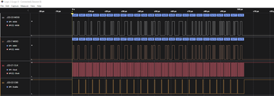
I can see J17-5 does clear then set again on each dropping edge of J17-6:
zoom in on one of the transfers:
So I am confident that the XBAR triggering the GPIO pins changing states does work.
- 新着としてマーク
- ブックマーク
- 購読
- ミュート
- RSS フィードを購読する
- ハイライト
- 印刷
- 不適切なコンテンツを報告
Test command '4' was made to prove that the SPI DMA transfer could be setup once and then just started using the commands:
dmaBASE->SERQ = DMA_SERQ_SERQ(0); // eDMA starts transfer RX channel
dmaBASE->SERQ = DMA_SERQ_SERQ(1); // eDMA starts transfer TX channel
This was used as a basis to apply to the multi chain operation after the GPIO dropping edge is first detected.
- 新着としてマーク
- ブックマーク
- 購読
- ミュート
- RSS フィードを購読する
- ハイライト
- 印刷
- 不適切なコンテンツを報告


