- Forums
- Product Forums
- General Purpose MicrocontrollersGeneral Purpose Microcontrollers
- i.MX Forumsi.MX Forums
- QorIQ Processing PlatformsQorIQ Processing Platforms
- Identification and SecurityIdentification and Security
- Power ManagementPower Management
- Wireless ConnectivityWireless Connectivity
- RFID / NFCRFID / NFC
- MCX Microcontrollers
- S32G
- S32K
- S32V
- MPC5xxx
- Other NXP Products
- S12 / MagniV Microcontrollers
- Powertrain and Electrification Analog Drivers
- Sensors
- Vybrid Processors
- Digital Signal Controllers
- 8-bit Microcontrollers
- ColdFire/68K Microcontrollers and Processors
- PowerQUICC Processors
- OSBDM and TBDML
- S32M
-
- Solution Forums
- Software Forums
- MCUXpresso Software and ToolsMCUXpresso Software and Tools
- CodeWarriorCodeWarrior
- MQX Software SolutionsMQX Software Solutions
- Model-Based Design Toolbox (MBDT)Model-Based Design Toolbox (MBDT)
- FreeMASTER
- eIQ Machine Learning Software
- Embedded Software and Tools Clinic
- S32 SDK
- S32 Design Studio
- GUI Guider
- Zephyr Project
- Voice Technology
- Application Software Packs
- Secure Provisioning SDK (SPSDK)
- Processor Expert Software
-
- Topics
- Mobile Robotics - Drones and RoversMobile Robotics - Drones and Rovers
- NXP Training ContentNXP Training Content
- University ProgramsUniversity Programs
- Rapid IoT
- NXP Designs
- SafeAssure-Community
- OSS Security & Maintenance
- Using Our Community
-
- Cloud Lab Forums
-
- Knowledge Bases
- ARM Microcontrollers
- i.MX Processors
- Identification and Security
- Model-Based Design Toolbox (MBDT)
- QorIQ Processing Platforms
- S32 Automotive Processing Platform
- Wireless Connectivity
- CodeWarrior
- MCUXpresso Suite of Software and Tools
- MQX Software Solutions
- RFID / NFC
-
- Home
- :
- i.MX处理器
- :
- i.MX RT Crossover MCUs Knowledge Base
- :
- RT600 MCUXpresso JLINK debug QSPI flash
RT600 MCUXpresso JLINK debug QSPI flash
RT600 MCUXpresso JLINK debug QSPI flash
RT600 MCUXpresso JLINK debug QSPI flash
RT600 MCUXpresso JLINK debug QSPI flash
1 Introduction
MIMXRT600-EVK is the NXP official board, which onboard flash is the external octal flash, the octal flash is connected to the RT685 flexSPI portB. In practical usage, the customer board may use other flash types, eg QSPI flash, and connect to the FlexSPI A port. Recently, nxp published one RT600 customer flash application note:
https://www.nxp.com/docs/en/application-note/AN13386.pdf
This document mainly gives the CMSIS DAP related flash algorithm usage, which modifies the option data to generate the new flash algo for the different flash types.
Some customer’s own board may use the RT600 QSPI flash+MCUXPresso+JLINK to debug the application code. Recently, one of the customers find on his own customer board, when they use debugger JLINK associated with the MCUXPresso download code to the RT600 QSPI flash, they meet download issues, but when using the CMSIS DAP as a debugger and the related QSPI cfx file, they can download OK. So this document mainly gives the experience of how to use the RT600, MCUXpresso IDE, and JLINK to download and debug the code which is located in the external QSPI flash.
2 JLINK driver prepare and test
MCUXpresso IDE use the JLINK download, it will call the JLINK driver related script and the flash algorithm, but to RT600, the JLINK driver will use the RT600 EVK flexSPI port B octal flash in default, so, if the customer board changes to other flexSPI port and to QSPI flash, they need to provide the related QSPI flash algorithm and script file, otherwise, even they can find the ARM CM33 core, the download will be still failed. If customers want to use the MCUXpresso IDE and the JLINK, they need to make sure the JLINK driver attached tool can do the external flash operation, eg, erase, read, write successfully at first. Now, give the JLINK driver related tool how to add the RT600 QSPI flash driver and script file.
2.1 JLINK driver install
Download the Segger JLINK driver from the following link:
https://www.segger.com/downloads/jlink/JLink_Windows_V754b_x86_64.exe
This document will use the jlink v7.54b to test, other version is similar.
Install the driver, the default driver install path is: C:\Program Files\SEGGER
2.2 Universal flashloader RT-UFL
RT-UFL v1.0 is a universal flashloader, which uses one .FLM file for all i.MXRT chips, and the different external flash, it is mainly used for the Segger JLINK debugger.
RT-UFL v1.0 downoad link:
https://github.com/JayHeng/RT-UFL/archive/refs/tags/v1.0.zip
Now, to the RT600 QSPI, give the related flash algo file patch.
Copy the following path file:
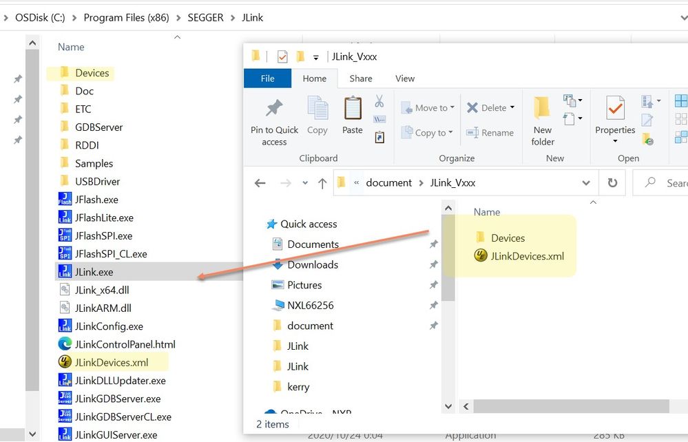
\RT-UFL-1.0\algo\SEGGER\JLink_Vxxx
To the JLINK install path:
\SEGGER\JLink
Then copy the content in file:
RT-UFL-master\test\SEGGER\JLink_Vxxx\Devices\NXP\iMXRT6xx\archive2\evkmimxrt685.JLinkScript
To replace the content in:
C:\Program Files\SEGGER\JLink\Devices\NXP\iMXRT_UFL\iMXRT6xx_CortexM33.JLinkScript
Otherwise, the MCUXpresso IDE debug reset button function will not work. So, need to add the JLINKScript code for ResetTarget, which will reset the external flash.
pic1
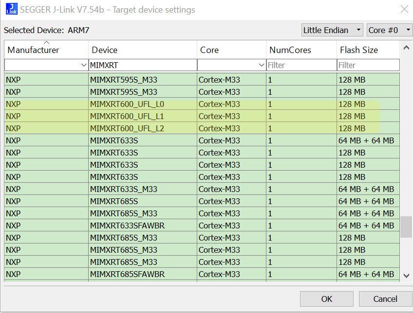
The RT-UFL provide 3 types download flash algo: MIMXRT600_UFL_L0, MIMXRT600_UFL_L1, MIMXRT600_UFL_L2.
Pic 2
_L0 used for the QSPI Flash and Octal Flash(page size 256 Bytes, sector size 4KB), _L1/2 used for the hyper flash(Page size 512 Bytes,Sector size 4KB/64KB). The JLINKDevices.xml content also can get the detail information. Different name will call different .FLM, the .FLM is the flash algorithm file, the source code can be found in RT-UFL v1.0, it will use different option0 option1 to configure the different external memory when the memory chip can support SFDP.
  <Device>
    <ChipInfo      Vendor="NXP"
                   Name="MIMXRT600_UFL_L0"
                   WorkRAMAddr="0x00000000"
                   WorkRAMSize="0x00480000"
                   Core="JLINK_CORE_CORTEX_M33"
                   JLinkScriptFile="Devices/NXP/iMXRT_UFL/iMXRT6xx_CortexM33.JLinkScript"
                   Aliases="MIMXRT633S; MIMXRT685S_M33"/>
    <FlashBankInfo Name="Octal Flash"
                   BaseAddr="0x08000000"
                   MaxSize="0x08000000"
                   Loader="Devices/NXP/iMXRT_UFL/MIMXRT_FLEXSPI_UFL_256B_4KB.FLM"
                   LoaderType="FLASH_ALGO_TYPE_OPEN" />
  </Device>
  <!------------------------>
  <Device>
    <ChipInfo      Vendor="NXP"
                   Name="MIMXRT600_UFL_L1"
                   WorkRAMAddr="0x00000000"
                   WorkRAMSize="0x00480000"
                   Core="JLINK_CORE_CORTEX_M33"
                   JLinkScriptFile="Devices/NXP/iMXRT_UFL/iMXRT6xx_CortexM33.JLinkScript"
                   Aliases="MIMXRT633S; MIMXRT685S_M33"/>
    <FlashBankInfo Name="Octal Flash"
                   BaseAddr="0x08000000"
                   MaxSize="0x08000000"
                   Loader="Devices/NXP/iMXRT_UFL/MIMXRT_FLEXSPI_UFL_512B_4KB.FLM"
                   LoaderType="FLASH_ALGO_TYPE_OPEN" />
  </Device>
  <!------------------------>
  <Device>
    <ChipInfo      Vendor="NXP"
                   Name="MIMXRT600_UFL_L2"
                   WorkRAMAddr="0x00000000"
                   WorkRAMSize="0x00480000"
                   Core="JLINK_CORE_CORTEX_M33"
                   JLinkScriptFile="Devices/NXP/iMXRT_UFL/iMXRT6xx_CortexM33.JLinkScript"
                   Aliases="MIMXRT633S; MIMXRT685S_M33"/>
    <FlashBankInfo Name="Octal Flash"
                   BaseAddr="0x08000000"
                   MaxSize="0x08000000"
                   Loader="Devices/NXP/iMXRT_UFL/MIMXRT_FLEXSPI_UFL_512B_64KB.FLM"
                   LoaderType="FLASH_ALGO_TYPE_OPEN" />
  </Device>
2.3 JLINK commander test
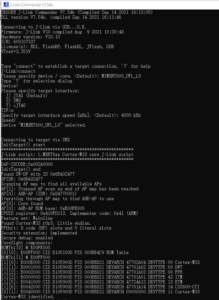
Please note, the device need to select as MIMXRT600_UFL_L0 when using the QSPI flash.
Pic 3
pic 4
Pic 5
We can find, the JLINK command can realize the external QSPI flash read, erase function.
2.4 Jflash Test
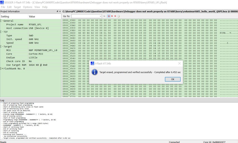
Operation steps: Target->connect->production programming
Pic 6
We can find, the Jflash also can realize the RT600 external QSPI flash erase and program.
Please note, not all the JLINK can support JFLASH, this document is using Segger JLINK plus.
3 MCUXpresso configuration and test
MCUXpresso: v11.4.0
SDK_2_10_0_EVK-MIMXRT685
MCUXPresso IDE import the SDK project, eg. Helloworld or led_output.
3.1 QSPI FCB configuration
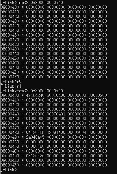
FCB is located from the flash offset address 0X08000400, which is used for the FlexSPI Nor boot configuration, the detailed content of the FCB can be found from the RT600 user manual Table 997. FlexSPI flash configuration block. Different external Flash, the configuration is different, if need to use the QSPI flash, the FCB should use the QSPI related configuration and its own LUT table.
Modify SDK project flash_config folder flash_config.c and flash_config.h, LUT contains fast read, status read, write enable, sector erase, block erase, page program, erase the whole chip. If the external QSPI flash command is different, the LUT command should be modified by following the flash datasheet mentioned related command.
const flexspi_nor_config_t flexspi_config = {
    .memConfig =
        {

	        .tag                  = FLASH_CONFIG_BLOCK_TAG,
	        .version              = FLASH_CONFIG_BLOCK_VERSION,
	        .readSampleClksrc=kFlexSPIReadSampleClk_LoopbackInternally,
	        .csHoldTime           = 3,
	        .csSetupTime          = 3,
	        .columnAddressWidth   = 0,
	        .deviceModeCfgEnable  = 0,
	        .deviceModeType       = 0,
	        .waitTimeCfgCommands  = 0,
	        .deviceModeSeq        = {.seqNum = 0,
	                                 .seqId  = 0,},
	        .deviceModeArg        = 0,
	        .configCmdEnable      = 0,
	        .configModeType       = {0},
	        .configCmdSeqs        = {0},
	        .configCmdArgs        = {0},
	        .controllerMiscOption = (0),
	        .deviceType           = 1,
	        .sflashPadType        = kSerialFlash_4Pads,
	        .serialClkFreq        = kFlexSpiSerialClk_133MHz,
	        .lutCustomSeqEnable   = 0,
	        .sflashA1Size         = BOARD_FLASH_SIZE,
	        .sflashA2Size         = 0,
	        .sflashB1Size         = 0,
	        .sflashB2Size         = 0,
	        .csPadSettingOverride = 0,
	        .sclkPadSettingOverride = 0,
	        .dataPadSettingOverride = 0,
	        .dqsPadSettingOverride  = 0,
	        .timeoutInMs            = 0,
	        .commandInterval        = 0,
	        .busyOffset             = 0,
	        .busyBitPolarity        = 0,
            .lookupTable =
                {
#if 0
                        [0]  = 0x08180403,
                        [1]  = 0x00002404,
                        [4]  = 0x24040405,
                        [12] = 0x00000604,
                        [20] = 0x081804D8,
                        [36] = 0x08180402,
                        [37] = 0x00002080,
                        [44] = 0x00000460,
#endif

// Fast Read
[4*0+0] = FLEXSPI_LUT_SEQ(CMD_SDR  ,  FLEXSPI_1PAD, 0xEB, RADDR_SDR, FLEXSPI_4PAD, 0x18),
[4*0+1] = FLEXSPI_LUT_SEQ(MODE4_SDR, FLEXSPI_4PAD, 0x00, DUMMY_SDR , FLEXSPI_4PAD, 0x09),
[4*0+2] = FLEXSPI_LUT_SEQ(READ_SDR , FLEXSPI_4PAD, 0x04, STOP_EXE  , FLEXSPI_1PAD, 0x00),

//read status
[4*1+0] = FLEXSPI_LUT_SEQ(CMD_SDR , FLEXSPI_1PAD, 0x05, READ_SDR, FLEXSPI_1PAD, 0x04),
//write Enable
[4*3+0] = FLEXSPI_LUT_SEQ(CMD_SDR, FLEXSPI_1PAD, 0x06, STOP_EXE, FLEXSPI_1PAD, 0),
// Sector Erase byte LUTs
[4*5+0] = FLEXSPI_LUT_SEQ(CMD_SDR, FLEXSPI_1PAD, 0x20, RADDR_SDR, FLEXSPI_1PAD, 0x18),
// Block Erase 64Kbyte LUTs
[4*8+0] = FLEXSPI_LUT_SEQ(CMD_SDR, FLEXSPI_1PAD, 0xD8, RADDR_SDR, FLEXSPI_1PAD, 0x18),
//Page Program - single mode
[4*9+0] = FLEXSPI_LUT_SEQ(CMD_SDR, FLEXSPI_1PAD, 0x02, RADDR_SDR, FLEXSPI_1PAD, 0x18),
[4*9+1] = FLEXSPI_LUT_SEQ(WRITE_SDR, FLEXSPI_1PAD, 0x04, STOP_EXE, FLEXSPI_1PAD, 0x0),
//Erase whole chip
[4*11+0]= FLEXSPI_LUT_SEQ(CMD_SDR, FLEXSPI_1PAD, 0x60, STOP_EXE, FLEXSPI_1PAD, 0),
              },
        },
    .pageSize           = 0x100,
    .sectorSize         = 0x1000,
    .ipcmdSerialClkFreq = 1,
    .isUniformBlockSize = 0,
    .blockSize          = 0x10000,
};
This code has been tested on the RT685+ QSPI flash MT25QL128ABA1ESE, the code boot is working.
3.2 Debug configuration
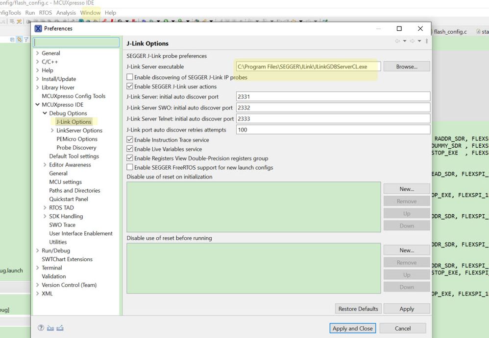
Configure the JLINK options in the MCUXpresso IDE as the JLINK driver: JLinkGDBServerCL.exe
Windows->preferences
Pic 7
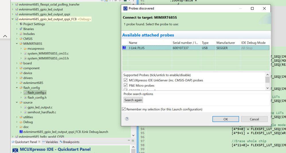
Press debug, generate .launch file.
Pic 8
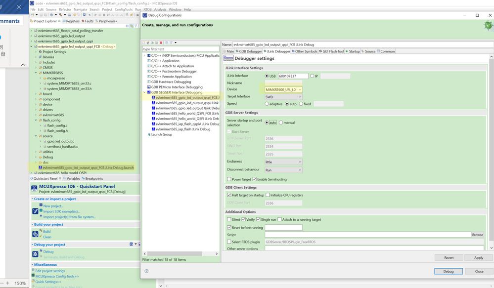
Run->Debug configurations
Pic 9
Choose the device as MIMXRT600_UFL_L0, if the SWD wire is long and not stable, also can define the speed as the fixed low frequency.
3.3 Download and debug test
Before download, need to check the RT685 ISP mode configuration, as this document is using the 4 wire QSPI and connect to the FlexSPI A port, so the ISP boot mode should be FlexSPI boot from Port A:
ISP2 PIO1_17 low, ISP1 PIO1_16 high, ISP0 PIO1_15 high
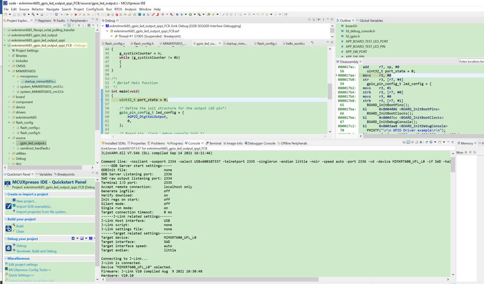
Click debug button, we can see the code enter the debug mode, and enter the main function, the code address is located in the flexSPI remap address.
Pic 10
Click run, we can find the RT685 pin P0_26 is toggling, and the UART interface also can printf information. The application code is working.
4 External SPI flash operation checking
To the customer designed board, normally we will use the JLINK command to check whether it can find the ARM core or not at first, make sure the RT chip can work, then will check the external flash operation or not.
4.1 SDK IAP flash code test
We can use the SDK related code to test the external flash operation or not at first, the SDK code path is:
SDK_2_10_0_EVK-MIMXRT685\boards\evkmimxrt685\driver_examples\iap\iap_flash
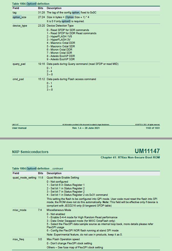
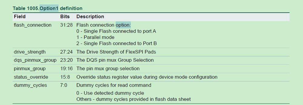
Then, check the external flash, and modify the code’s related option0, option1 to match the external flash. About the option 0 and option1 definition, we can find it from the RT600 user manual Table 1004.Option0 definition and Table 1005.Option1 definition
Pic 11
Pic 12
To the external QSPI flash which is connected to the FLexSPI portA, we can modify the option to the following code:
option.option0.U = 0xC0000001;//EXAMPLE_NOR_FLASH;
option.option1.U = 0x00000000;//EXAMPLE_NOR_FLASH_OPTION1;
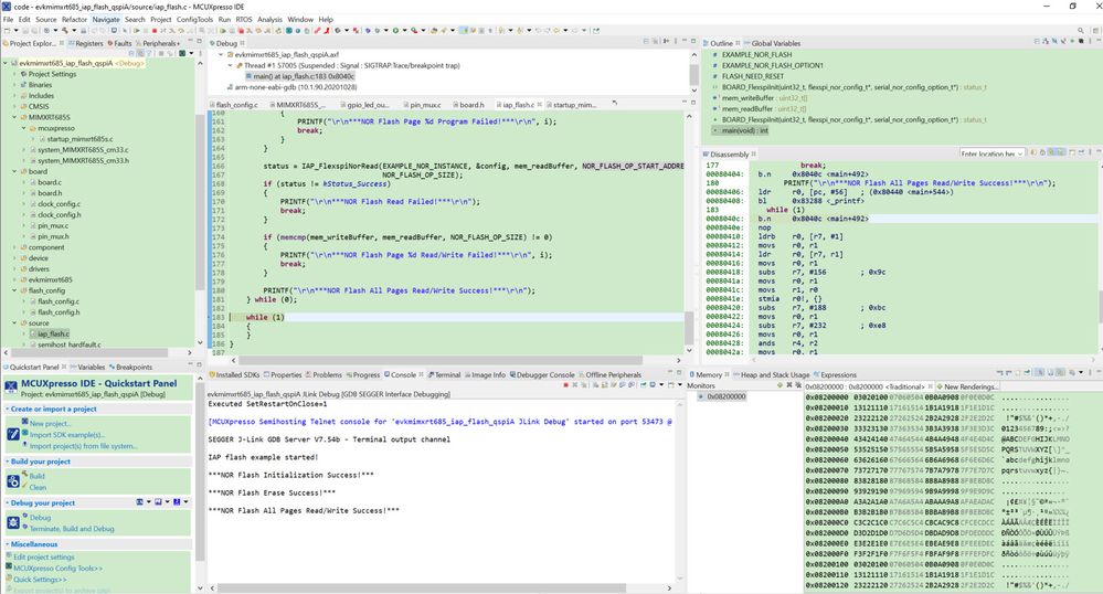
Then burn the IAP_flash project to the RT685 internal RAM, debug to run it.
Pic 13
We can find, the external QSPI flash initialization, erase, read and write all works, and the memory also can find the correct data.
4.2 MCUBootUtility test
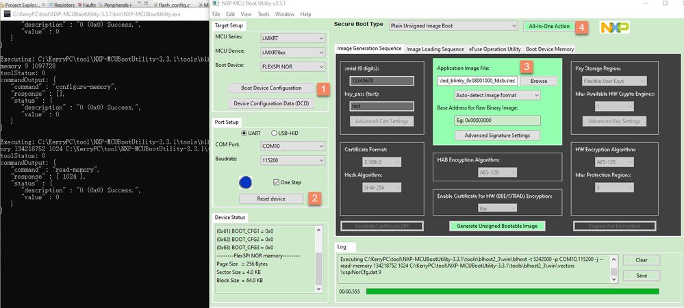
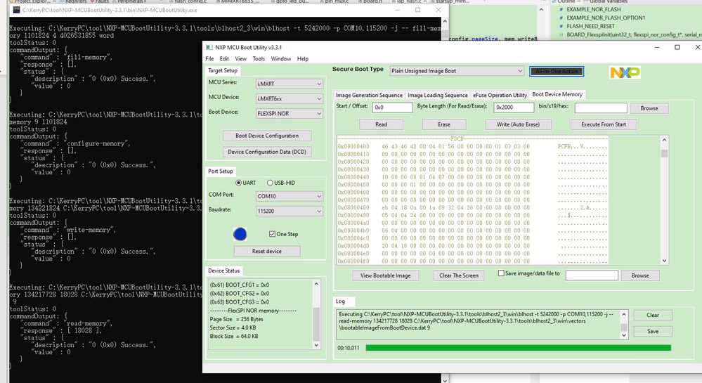
Chip enter the ISP mode, then use the MCUBootUtility tool to connect the RT685 and QSPI flash, to do the application code program and read test.
ISP mode:ISP2:high, ISP1: high ISP0 low
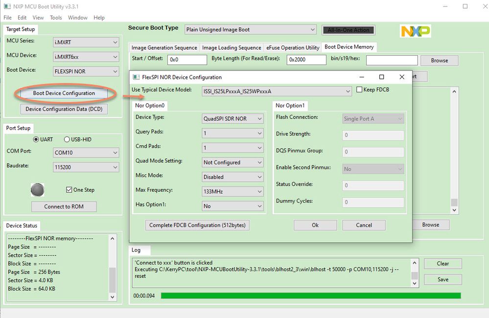
Configure FlexSPI NOR Device Configuration as QSPI, we can use the template: ISSI_IS25LPxxxA_IS25WPxxxA.
Pic 14
Click connect to ROM button, check whether it can recognize the external flash:
Pic 15
After connection, we can use the tool attached RT685 image to download:
NXP-MCUBootUtility-3.3.1\apps\NXP_MIMXRT685-EVK_Rev.E\led_blinky_0x08001000_fdcb.srec
Pic 16
We can find, the connection, erase, program and read are all work, it also indicates the RT685+external QSPI flash is working. Then can go to debug it with IDE and debugger.
