
- NXP Forums
- Product Forums
- General Purpose MicrocontrollersGeneral Purpose Microcontrollers
- i.MX Forumsi.MX Forums
- QorIQ Processing PlatformsQorIQ Processing Platforms
- Identification and SecurityIdentification and Security
- Power ManagementPower Management
- MCX Microcontrollers
- S32G
- S32K
- S32V
- MPC5xxx
- Other NXP Products
- Wireless Connectivity
- S12 / MagniV Microcontrollers
- Powertrain and Electrification Analog Drivers
- Sensors
- Vybrid Processors
- Digital Signal Controllers
- 8-bit Microcontrollers
- ColdFire/68K Microcontrollers and Processors
- PowerQUICC Processors
- OSBDM and TBDML
-
- Solution Forums
- Software Forums
- MCUXpresso Software and ToolsMCUXpresso Software and Tools
- CodeWarriorCodeWarrior
- MQX Software SolutionsMQX Software Solutions
- Model-Based Design Toolbox (MBDT)Model-Based Design Toolbox (MBDT)
- FreeMASTER
- eIQ Machine Learning Software
- Embedded Software and Tools Clinic
- S32 SDK
- S32 Design Studio
- Vigiles
- GUI Guider
- Zephyr Project
- Voice Technology
- Application Software Packs
- Secure Provisioning SDK (SPSDK)
- Processor Expert Software
-
- Topics
- Mobile Robotics - Drones and RoversMobile Robotics - Drones and Rovers
- NXP Training ContentNXP Training Content
- University ProgramsUniversity Programs
- Rapid IoT
- NXP Designs
- SafeAssure-Community
- OSS Security & Maintenance
- Using Our Community
-
- Cloud Lab Forums
-
- Home
- :
- i.MX Forums
- :
- i.MX Processors
- :
- what is the function of flash.ld and ram.ld files about SDK_2_11_1_EVK-MIMXRT595?
what is the function of flash.ld and ram.ld files about SDK_2_11_1_EVK-MIMXRT595?
- Subscribe to RSS Feed
- Mark Topic as New
- Mark Topic as Read
- Float this Topic for Current User
- Bookmark
- Subscribe
- Mute
- Printer Friendly Page
- Mark as New
- Bookmark
- Subscribe
- Mute
- Subscribe to RSS Feed
- Permalink
- Report Inappropriate Content
Hi
There are MIMXRT595Sxxxx_cm33_flash.ld and MIMXRT595Sxxxx_cm33_ram.ld files about examples.
1. What is the function of these two files and why are these two link files needed?
2. When BOOT rom loads images, how do they work and which one works first?
Compilation tool: GCC
Solved! Go to Solution.
- Mark as New
- Bookmark
- Subscribe
- Mute
- Subscribe to RSS Feed
- Permalink
- Report Inappropriate Content
Hi @Dave_SU ,
You are welcome!
If your question is solved, please help me to mark the correct answer, just to close this case, any new issues in the future, welcome to create the new question post, we will help you in your new post.
Best Regards,
kerry
- Mark as New
- Bookmark
- Subscribe
- Mute
- Subscribe to RSS Feed
- Permalink
- Report Inappropriate Content
Hi @Dave_SU ,
Thanks you for your interest in the NXP MIMXRT product, I would like to provide service for you.
Answer your 2 questions:
1. What is the function of these two files and why are these two link files needed?
=> MIMXRT595Sxxxx_cm33_flash.ld: the image will generate to the flash address
MIMXRT595Sxxxx_cm33_ram.ld: the image will generate to the internal RAM address
the flash.ld normally to put the code in the external flash, as you know, the RT595 support the XIP, it can run the code in the external flash directly.
the ram.ld normally to put the code in the internal RAM code, as you know, the code will run in the internal RAM directly.
2. When BOOT rom loads images, how do they work and which one works first?
=> As you know, the BOOT ROM will read the FCB at first, it will check the APP address, if it is the flash, then jump to the flash, if it is the RAM, copy the code from the flash to RAM, then jump to RAM.
Wish it helps you!
Best Regards,
kerry
- Mark as New
- Bookmark
- Subscribe
- Mute
- Subscribe to RSS Feed
- Permalink
- Report Inappropriate Content
Dear @kerryzhou
Thank you for your reply. There are still some questions that need your help.
Q1. As you mentioned, if my board is set to FlexSPI BOOT mode and XIP is not enabled, the flash.ld file will not be used, right?
BOOT set : PRIMARY_BOOT_SRC bits[3:0] is not set(default value is b'0000), ISP_Pin[2:0] is set '011'
2. When BOOT rom loads images, how do they work and which one works first?
=> As you know, the BOOT ROM will read the FCB at first, it will check the APP address, if it is the flash, then jump to the flash, if it is the RAM, copy the code from the flash to RAM, then jump to RAM.
Q2.How does BOOT ROM check the address of APP, and how to distinguish whether it is flash or RAM?
Q3.Does the SDK have a demo about XIP?
- Mark as New
- Bookmark
- Subscribe
- Mute
- Subscribe to RSS Feed
- Permalink
- Report Inappropriate Content
Hi @kerryzhou
Thank you for your reply.
Do you know the srec file?
[Dave]: I don't know it.
All the SDK flash code is the XIP code in default.
[Dave]: It's so amazing to me. When I debug the SDK PCA9420 demo(\SDK_2_11_1_EVK-MIMXRT595\boards\evkmimxrt595\driver_examples\pca9420, The bin file attached), I found that the place where 0x20280000 of SRM starts and the place where 0x00280000 starts, the stored data is the same. Why they are same?
Memory partition:
MEMORY
{
m_flash (RX) : ORIGIN = 0x08000000, LENGTH = 0x00300000
m_interrupts (RX) : ORIGIN = 0x00280000, LENGTH = 0x00000180
m_text (RX) : ORIGIN = 0x00280180, LENGTH = 0x0013FE80
m_data (RW) : ORIGIN = 0x203C0000, LENGTH = 0x00140000
m_usb_sram (RW) : ORIGIN = 0x40140000, LENGTH = 0x00004000
}
In this case, I thank the demo run as non-XIP. As the picture(attached) shows, Is it correct that I understand the process of bootimage loading?
- Mark as New
- Bookmark
- Subscribe
- Mute
- Subscribe to RSS Feed
- Permalink
- Report Inappropriate Content
Hi @Dave_SU
Your interrupt is in the RAM:
m_interrupts (RX) : ORIGIN = 0x00280000, LENGTH = 0x00000180
So, your code is the Non-XIP, it will run in the internal RAM.
Your picture and your understand is correct.
0x20280000 and 0x00280000 is the different RAM address.
It is determined by your code assignment.
Your mentioned sample code, check the flash.ld:
define symbol m_interrupts_start = 0x08001000;
define symbol m_interrupts_end = 0x0800117F;
define symbol m_text_start = 0x08001180;
define symbol m_text_end = 0x081FFFFF;
define symbol m_interrupts_ram_start = 0x20280000;
define symbol m_interrupts_ram_end = 0x20280000 + __ram_vector_table_offset__;
here, it will boot from the external flash, XIP, then it will copy the interrupt from external flash address to the internal RAM by the app code, this still the XIP code, as the code is run from external flash.
ram.ld:
define symbol m_interrupts_start = 0x00280000;
define symbol m_interrupts_end = 0x0028017F;
define symbol m_text_start = 0x00280180;
define symbol m_text_end = 0x003BFFFF;
This interrupt is directly in the internal RAM, ROM will jump to the internal RAM directly, so it is non-xip.
Best Regards,
Kerry
- Mark as New
- Bookmark
- Subscribe
- Mute
- Subscribe to RSS Feed
- Permalink
- Report Inappropriate Content
Hi @kerryzhou
I'm not very clear about the process.
As we know, there two ld files(flash.ld and ram.ld) in SDK demo.
According to your explanation, I understand the process like this, is it correct?
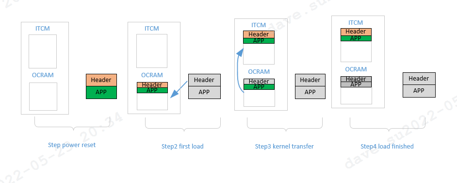
Step 1:
BOOT ROM loads the bootable image from the external flash according to the flash.ld file.
After BOOT ROM finished init FlexSPI, then transfers the control to the user app code。At this time,
RT595 executes XIP mode in external flash, APP loads the bootable image to ram(the target address is defined by flash ram.ld, it's 0x20280000).
Step 2:
The kernel copies the entire bootable image to the target address (0x00280000)defined by ram.ld,
Step 3:
RT595 runs the app in the SARM. And the app runs as non-xip mode.
If so, it is very difficult to understand, in the non-XIP mode, why the BOOT ROM does not directly copy the code to the target RAM(defined by ram.ld file), it is necessary to XIP first, and then switch to the non-XIP mode.
- Mark as New
- Bookmark
- Subscribe
- Mute
- Subscribe to RSS Feed
- Permalink
- Report Inappropriate Content
Hi @Dave_SU ,
Please read this application note, which may useful to your understanding:
https://www.nxp.com.cn/docs/en/application-note/AN12773.pdf
If your execute code is directly in the flash, then it is the XIP.
If your execute code just download to the external flash, but the image still run in the internal RAM, then it is non-XIP.
flash.ld is used to generate the code which is located in the external flash.
ram.ld is used to generate the code which is located in the internal RAM, but you still can download it to the external flash, as the ROM will detect it, and copy it to it's real RAM area.
To you question: in the non-XIP mode, why the BOOT ROM does not directly copy the code to the target RAM(defined by ram.ld file)
Of course ROM will copy the code to the target RAM, download to flash just used for boot, as you know, RAM code will be disappear after POR, so flash need to store it at first.
I think, you can use the blhost method download the different .ld generated image, then it will helps your understanding.
Wish it helps you!
Best Regards,
Kerry
- Mark as New
- Bookmark
- Subscribe
- Mute
- Subscribe to RSS Feed
- Permalink
- Report Inappropriate Content
Hi @kerryzhou
Thanks for your reply, it gave me a clear understanding of this process.
One more question, the file(https://www.nxp.com.cn/docs/en/application-note/AN12773.pdf) about RT600, is it the same boot process as RT500? Do you have documentation for RT500.
- Mark as New
- Bookmark
- Subscribe
- Mute
- Subscribe to RSS Feed
- Permalink
- Report Inappropriate Content
Hi @Dave_SU
Don't worry, RT500 totally the same operation as the RT600, you can refer to that AN.
BTW, a good tool recommended to you:
https://github.com/JayHeng/NXP-MCUBootUtility/releases/tag/v3.5.0
the related user manual is:
https://github.com/JayHeng/NXP-MCUBootUtility
This will help you download code, and readout the memory, helps your understanding.
Wish it helps you!
Best Regards,
Kerry
- Mark as New
- Bookmark
- Subscribe
- Mute
- Subscribe to RSS Feed
- Permalink
- Report Inappropriate Content
- Mark as New
- Bookmark
- Subscribe
- Mute
- Subscribe to RSS Feed
- Permalink
- Report Inappropriate Content
Hi @Dave_SU ,
You are welcome!
If your question is solved, please help me to mark the correct answer, just to close this case, any new issues in the future, welcome to create the new question post, we will help you in your new post.
Best Regards,
kerry
- Mark as New
- Bookmark
- Subscribe
- Mute
- Subscribe to RSS Feed
- Permalink
- Report Inappropriate Content
Hi @Dave_SU ,
Q1. As you mentioned, if my board is set to FlexSPI BOOT mode and XIP is not enabled, the flash.ld file will not be used, right?
BOOT set : PRIMARY_BOOT_SRC bits[3:0] is not set(default value is b'0000), ISP_Pin[2:0] is set '011'
2. When BOOT rom loads images, how do they work and which one works first?
=> As you know, the BOOT ROM will read the FCB at first, it will check the APP address, if it is the flash, then jump to the flash, if it is the RAM, copy the code from the flash to RAM, then jump to RAM.
=>kerry: when you generate the code, the ld file is not related to the boot now.
Do you know the srec file? If you generate the .srec file, you can find your app address, the address will let you see the memory area, about the address memory map, you can check the RT595 RM:

flash is the XIP code, RAM is the non-XIP code.
Q2.How does BOOT ROM check the address of APP, and how to distinguish whether it is flash or RAM?
=>kerry: check the resetISR address
Flash generated code, you can see the resetISR is in the flash:

RAM code:
resetISR is in the RAM address

Q3.Does the SDK have a demo about XIP?
=>All the SDK flash code is the XIP code in default.
Wish it helps you!
Best Regards,
Kerry