- Forums
- Product Forums
- General Purpose MicrocontrollersGeneral Purpose Microcontrollers
- i.MX Forumsi.MX Forums
- QorIQ Processing PlatformsQorIQ Processing Platforms
- Identification and SecurityIdentification and Security
- Power ManagementPower Management
- Wireless ConnectivityWireless Connectivity
- RFID / NFCRFID / NFC
- MCX Microcontrollers
- S32G
- S32K
- S32V
- MPC5xxx
- Other NXP Products
- S12 / MagniV Microcontrollers
- Powertrain and Electrification Analog Drivers
- Sensors
- Vybrid Processors
- Digital Signal Controllers
- 8-bit Microcontrollers
- ColdFire/68K Microcontrollers and Processors
- PowerQUICC Processors
- OSBDM and TBDML
- S32M
-
- Solution Forums
- Software Forums
- MCUXpresso Software and ToolsMCUXpresso Software and Tools
- CodeWarriorCodeWarrior
- MQX Software SolutionsMQX Software Solutions
- Model-Based Design Toolbox (MBDT)Model-Based Design Toolbox (MBDT)
- FreeMASTER
- eIQ Machine Learning Software
- Embedded Software and Tools Clinic
- S32 SDK
- S32 Design Studio
- GUI Guider
- Zephyr Project
- Voice Technology
- Application Software Packs
- Secure Provisioning SDK (SPSDK)
- Processor Expert Software
-
- Topics
- Mobile Robotics - Drones and RoversMobile Robotics - Drones and Rovers
- NXP Training ContentNXP Training Content
- University ProgramsUniversity Programs
- Rapid IoT
- NXP Designs
- SafeAssure-Community
- OSS Security & Maintenance
- Using Our Community
-
- Cloud Lab Forums
-
- Knowledge Bases
- ARM Microcontrollers
- i.MX Processors
- Identification and Security
- Model-Based Design Toolbox (MBDT)
- QorIQ Processing Platforms
- S32 Automotive Processing Platform
- Wireless Connectivity
- CodeWarrior
- MCUXpresso Suite of Software and Tools
- MQX Software Solutions
- RFID / NFC
-
- Home
- :
- i.MX Forums
- :
- i.MX Processors
- :
- Re: iMX6 DDR3 Calibration Failure
iMX6 DDR3 Calibration Failure
- Subscribe to RSS Feed
- Mark Topic as New
- Mark Topic as Read
- Float this Topic for Current User
- Bookmark
- Subscribe
- Mute
- Printer Friendly Page
iMX6 DDR3 Calibration Failure
- Mark as New
- Bookmark
- Subscribe
- Mute
- Subscribe to RSS Feed
- Permalink
- Report Inappropriate Content
Hi,
I am trying to run DDR3 calibration for imx6 quad processor (MCIMX6Q5EYM10AC) with 4 memory chips (MT41K256M16TW-107) in flyby topology using only CS0. I am running V3.0 of the test script (aid document attached). Please see log below
============================================
DDR Stress Test (3.0.0)
Build: Dec 14 2018, 14:12:06
NXP Semiconductors.
============================================
============================================
Chip ID
CHIP ID = i.MX6 Dual/Quad (0x63)
Internal Revision = TO1.2
============================================
============================================
Boot Configuration
SRC_SBMR1(0x020d8004) = 0x00000000
SRC_SBMR2(0x020d801c) = 0x30000001
============================================
ARM Clock set to 1GHz
============================================
DDR configuration
BOOT_CFG3[5-4]: 0x00, Single DDR channel.
DDR type is DDR3
Data width: 64, bank num: 8
Row size: 15, col size: 10
Chip select CSD0 is used
Density per chip select: 2048MB
============================================
Current Temperature: 43
============================================
DDR Freq: 396 MHz
ddr_mr1=0x00000000
Start write leveling calibration...
running Write level HW calibration
MPWLHWERR register read out for factory diagnostics:
MPWLHWERR PHY0 = 0x00003878
HW WL cal status: no suitable delay value found for byte 2
HW WL cal status: no suitable delay value found for byte 3
MPWLHWERR PHY1 = 0x1e1e1e3c
Write leveling calibration completed but failed, the following results were found:
MMDC_MPWLDECTRL0 ch0 (0x021b080c) = 0x0043004E
MMDC_MPWLDECTRL1 ch0 (0x021b0810) = 0x001F001F
MMDC_MPWLDECTRL0 ch1 (0x021b480c) = 0x001D0030
MMDC_MPWLDECTRL1 ch1 (0x021b4810) = 0x00110015
Write DQS delay result:
Write DQS0 delay: 78/256 CK
Write DQS1 delay: 67/256 CK
Write DQS2 delay: 31/256 CK
Write DQS3 delay: 31/256 CK
Write DQS4 delay: 48/256 CK
Write DQS5 delay: 29/256 CK
Write DQS6 delay: 21/256 CK
Write DQS7 delay: 17/256 CK
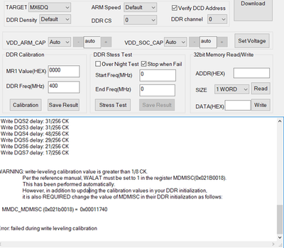
WARNING: write-leveling calibration value is greater than 1/8 CK.
Per the reference manual, WALAT must be set to 1 in the register MDMISC(0x021B0018).
This has been performed automatically.
However, in addition to updating the calibration values in your DDR initialization,
it is also REQUIRED change the value of MDMISC in their DDR initialization as follows:
MMDC_MDMISC (0x021b0018) = 0x00011740
Error: failed during write leveling calibration
Please help.
Regards,
Sreedhar
- Mark as New
- Bookmark
- Subscribe
- Mute
- Subscribe to RSS Feed
- Permalink
- Report Inappropriate Content
Density per chip select: 2048MB
this does not match with your configuration.
- Mark as New
- Bookmark
- Subscribe
- Mute
- Subscribe to RSS Feed
- Permalink
- Report Inappropriate Content
The most likely cause of the issue is the PCB-level design issue e.g. trace
length mismatch, impedance mismatch etc. Check your PCB design against the
recommendations, given in the Hardware Development Guide for i.MX 6QuadPlus,
6Quad, 6DualPlus, 6Dual, 6DualLite, 6Solo Families of Applications Processors
document, available on the processor's Documentation web page:
Best Regards,
Artur
- Mark as New
- Bookmark
- Subscribe
- Mute
- Subscribe to RSS Feed
- Permalink
- Report Inappropriate Content
Any help is high appreciated.
Regards,
Sreedhar Nair
