- Forums
- Product Forums
- General Purpose MicrocontrollersGeneral Purpose Microcontrollers
- i.MX Forumsi.MX Forums
- QorIQ Processing PlatformsQorIQ Processing Platforms
- Identification and SecurityIdentification and Security
- Power ManagementPower Management
- Wireless ConnectivityWireless Connectivity
- RFID / NFCRFID / NFC
- MCX Microcontrollers
- S32G
- S32K
- S32V
- MPC5xxx
- Other NXP Products
- S12 / MagniV Microcontrollers
- Powertrain and Electrification Analog Drivers
- Sensors
- Vybrid Processors
- Digital Signal Controllers
- 8-bit Microcontrollers
- ColdFire/68K Microcontrollers and Processors
- PowerQUICC Processors
- OSBDM and TBDML
- S32M
-
- Solution Forums
- Software Forums
- MCUXpresso Software and ToolsMCUXpresso Software and Tools
- CodeWarriorCodeWarrior
- MQX Software SolutionsMQX Software Solutions
- Model-Based Design Toolbox (MBDT)Model-Based Design Toolbox (MBDT)
- FreeMASTER
- eIQ Machine Learning Software
- Embedded Software and Tools Clinic
- S32 SDK
- S32 Design Studio
- GUI Guider
- Zephyr Project
- Voice Technology
- Application Software Packs
- Secure Provisioning SDK (SPSDK)
- Processor Expert Software
-
- Topics
- Mobile Robotics - Drones and RoversMobile Robotics - Drones and Rovers
- NXP Training ContentNXP Training Content
- University ProgramsUniversity Programs
- Rapid IoT
- NXP Designs
- SafeAssure-Community
- OSS Security & Maintenance
- Using Our Community
-
- Cloud Lab Forums
-
- Knowledge Bases
- ARM Microcontrollers
- i.MX Processors
- Identification and Security
- Model-Based Design Toolbox (MBDT)
- QorIQ Processing Platforms
- S32 Automotive Processing Platform
- Wireless Connectivity
- CodeWarrior
- MCUXpresso Suite of Software and Tools
- MQX Software Solutions
- RFID / NFC
-
- Home
- :
- i.MX フォーラム
- :
- i.MXプロセッサ
- :
- LPSPI & eDMA master RT1060
LPSPI & eDMA master RT1060
- RSS フィードを購読する
- トピックを新着としてマーク
- トピックを既読としてマーク
- このトピックを現在のユーザーにフロートします
- ブックマーク
- 購読
- ミュート
- 印刷用ページ
LPSPI & eDMA master RT1060
- 新着としてマーク
- ブックマーク
- 購読
- ミュート
- RSS フィードを購読する
- ハイライト
- 印刷
- 不適切なコンテンツを報告
I'm trying to configure the LPSPI peripheral in master mode using eDMA on the RT1062 evaluation kit, but I'm not getting the waveforms I expect.
I want to transfer 6144 bytes without any software intervention. The transfer should be broken into 512 frames of 12 bytes each (ie chip select should go low for 12 bytes). Each frame should be separated by 5us.
I've configured the LPSPI and eDMA peripherals using the MCUXpresso Peripheral Config tool. I set the 'Bits Per Frame' setting to 96 (ie 12 bytes * 8 bits/byte). Although I set the 'Delay Between Transfers' to 5000 ns, I'm seeing a waveform that has only 2.4us between transfers. Increasing the delay to 10000 ns makes no difference, the delay seems to be maxed out at 2.4us.
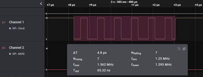
Instead of using the 'Delay Between Transfers' setting, I also tried using the 'Periodic Trigger Enable' in the LPSPI > eDMA > Transmit settings. I configured the PIT channel 1 with a 5us setting. This resulted in the very confusing waveform shown below. It appears that the LPSPI peripheral makes 3 transfers of 4 bytes, with each transfer separated by 5us, but it's all within a single SPI frame. This is not what I need. Rant: I can't imagine anyone would need such a configuration!
Can someone help point me in the right direction?
Tools & hardware: MIMXRT1060-EVKB, MCUXpresso 11.6.0_8187, SDK 2.12.0 (611 2022-07-14)
- 新着としてマーク
- ブックマーク
- 購読
- ミュート
- RSS フィードを購読する
- ハイライト
- 印刷
- 不適切なコンテンツを報告
Hey Mike, I've made some progress on this issue, but I still need your help.
I attached the evkmimxrt1060_iled_blinky example project that I modified to transmit data via the LPSPI driver. There are only a few lines of code that I added in led_blinky.c. Note the lpspi_tx_test() function call in main().
I had to enable the MCUXpresso Peripheral Config tool, because this project didn't have it enabled by default.
I modified the clock configuration via the MCUXpresso Clock Config tool so that the LPSPI functional clock is 96MHz, which is driven by the PLL3 PFD0 clock source.
One other thing to note, I modified the drivers/fsl_lpspi.c so that the TCR.PRESCALE = 1, CCR.SCKDIV = 0, CCR.DBT = 238, CCR.PCSSCK = 23, and CCR.SCKPCS = 23. You can disable these edits by removing the #define GLAUKOS_EDITS at the top of the file.
With these changes I see an SPI clock of 20.8333MHz and a delay between transfers of 6us. This is incorrect. According to the setting above, the clock rate should be 24MHz (96MHz / 2 from PRESCALE / 2 from SCKDIV). The delay between transfers should be 5us (238 + 2) / (96MHz / 2 from PRESCALE).
Not sure if this is relevant or not, but I noticed something interesting, which might mean there's something wrong in the MCXpresso Clock Configuration tool. If we back calculate the PLL3 PFD0 clock using the measured SPI clock, we find that PLL3 PFD0 is exactly 500MHz, when it should be 576MHz. (20.833MHz * 2 from TCR.PRESCALE * 2 from CCR.SCKDIV * 6 from CCM.LPSPI_PODF).
- 新着としてマーク
- ブックマーク
- 購読
- ミュート
- RSS フィードを購読する
- ハイライト
- 印刷
- 不適切なコンテンツを報告
Hi,
First of all, sorry for the later reply.
I did a test with your attached <evkmimxrt1060_iled_blinky> project and measure the SPI signal at RT1060 EVK board.
The SPI signal looks quite strange:
LPSPI clock source as you setting at 96MHz.
While it looks SPI duty cycle is not 50% and the SPI transmit is 7bit not 8bit.
If customer had referred the <evkmimxrt1060_lpspi_edma_b2b_transfer_master> about LPSI eDMA transfer.
Thanks for the attention.
Mike
- 新着としてマーク
- ブックマーク
- 購読
- ミュート
- RSS フィードを購読する
- ハイライト
- 印刷
- 不適切なコンテンツを報告
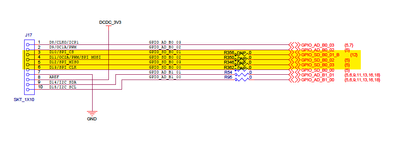
@Hui_Ma thanks for the reply. The scope capture of the SPI signals you posted does indeed look very strange. Why do you think your capture looks so very different than mine? Are you sure you've configured your board properly? I'm probing the SPI bus using pins on J17. I had to populate R356, R350, R346, and R362.
I took a look at the evkmimxrt1060_lpspi_edma_b2b_transfer_master example project as you suggested, but this example only transfers one frame of SPI data containing 64 bytes and then generates a transfer complete interrupt. I want to transfer multiple frames of data without any software intervention.
Perhaps you could modify the evkmimxrt1060_lpspi_edma_b2b_transfer_master project to send 2 frames of 64 bytes without generating an interrupt in between them and send it to me? The SPI clock rate should be 24MHz. That would be very helpful, thanks!
- 新着としてマーク
- ブックマーク
- 購読
- ミュート
- RSS フィードを購読する
- ハイライト
- 印刷
- 不適切なコンテンツを報告
Hi,
I am using the J24 to measure the LPSPI1 signals, that could be the root cause.
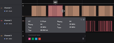
I did another test with evkmimxrt1060_lpspi_edma_b2b_transfer_master project, when I change the bitsPerFrame setting could get below signals (SPI baud rate: 20MHz):
The each transfer internal could be change by EXAMPLE_LPSPI_CLOCK_SOURCE_DIVIDER macro definition.
/* Clock divider for master lpspi clock source */
#define EXAMPLE_LPSPI_CLOCK_SOURCE_DIVIDER (0U)
If I change the EXAMPLE_LPSPI_CLOCK_SOURCE_DIVIDER value to 3, then the interval value would change to 2.1us
I add the transfer size to 128 bytes. When whole transfer done will trigger the LPSPI master callback interrupt.
I attached my test project for your reference.
Wish it helps.
Mike
- 新着としてマーク
- ブックマーク
- 購読
- ミュート
- RSS フィードを購読する
- ハイライト
- 印刷
- 不適切なコンテンツを報告
Thanks @Hui_Ma, but this is not what I asked for. The code you provided makes two transfers, which means two interrupts are generated; one for each transfer.
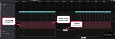
Furthermore, the time between the two frames is indeterminate, but it needs to be 5us. This was stated in my original question. You will need to probe the chip select (CS) line in order to see this timing on your scope.
The SPI clock should be 24MHz and there should not be any delay between the bytes in the frame. Here you can see 2.128us between the transfer of each byte.
This is what the transfer should look like, except that the time between frames should be 5us and the SCK should be 24MHz.
How do I achieve this with ONE call of LPSPI_MasterTransferEDMA?
- 新着としてマーク
- ブックマーク
- 購読
- ミュート
- RSS フィードを購読する
- ハイライト
- 印刷
- 不適切なコンテンツを報告
Hi,
I will work for this LPSPI eDMA transfer example, which would take sometime and I will update here when there with any progress. Thank you for the patience.
Mike
- 新着としてマーク
- ブックマーク
- 購読
- ミュート
- RSS フィードを購読する
- ハイライト
- 印刷
- 不適切なコンテンツを報告
@Hui_Ma I believe I've found the answer to my own question.
It appears that the Clock Diagram in the MCXpresso Clock Config tool does not accurately represent the code that it generated.
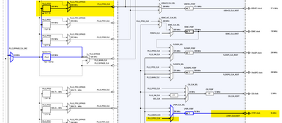
Here in the Clock Diagram we can see that the LPSPI_CLK_ROOT is derived from the PLL3 PFD0 clock. The PLL3 PFD0 clock is configured with a divider of 15, so that the output is 576MHz. With an LPSPI_PODF divider of 6, that results in the LPSPI clock = 96MHz.
However, when we look at the BOARD_BootClockRUN function in the clock_config.c file that is generated by the tool there are defines which are preventing the PLL3 PFD0 configuration from being applied.This means that the LPSPI clock is not 96MHz as expected, which then means any SCK and DBT configuration will also be wrong.
It would be nice if the MCUXpresso Clock Config tool indicated this is some way from the GUI rather than forcing users to dig through generated code and register settings!
The solution that worked for me was to use the PLL2 PFD2 as the clock source for the LPSPI peripheral. I set the PLL2 PFD2 divider to 33 and the LPSPI PODF divider to 3 so that the LPSPI clock is actually 96MHz.
- 新着としてマーク
- ブックマーク
- 購読
- ミュート
- RSS フィードを購読する
- ハイライト
- 印刷
- 不適切なコンテンツを報告
Hi,
You are correct. The BOARD_BootClockRUN() function mask the USB1 PLL configuration.
Thank you for the MCUXpresso Config tool related suggeation, I will forward to SDK software team.
best regards,
Mike
- 新着としてマーク
- ブックマーク
- 購読
- ミュート
- RSS フィードを購読する
- ハイライト
- 印刷
- 不適切なコンテンツを報告
Hi,
First of all, sorry for the later reply.
Could you help to provide your test code? Then we would like to do an onsite test. Thanks.
Mike


