- Forums
- Product Forums
- General Purpose MicrocontrollersGeneral Purpose Microcontrollers
- i.MX Forumsi.MX Forums
- QorIQ Processing PlatformsQorIQ Processing Platforms
- Identification and SecurityIdentification and Security
- Power ManagementPower Management
- Wireless ConnectivityWireless Connectivity
- RFID / NFCRFID / NFC
- Advanced AnalogAdvanced Analog
- MCX Microcontrollers
- S32G
- S32K
- S32V
- MPC5xxx
- Other NXP Products
- S12 / MagniV Microcontrollers
- Powertrain and Electrification Analog Drivers
- Sensors
- Vybrid Processors
- Digital Signal Controllers
- 8-bit Microcontrollers
- ColdFire/68K Microcontrollers and Processors
- PowerQUICC Processors
- OSBDM and TBDML
- S32M
- S32Z/E
-
- Solution Forums
- Software Forums
- MCUXpresso Software and ToolsMCUXpresso Software and Tools
- CodeWarriorCodeWarrior
- MQX Software SolutionsMQX Software Solutions
- Model-Based Design Toolbox (MBDT)Model-Based Design Toolbox (MBDT)
- FreeMASTER
- eIQ Machine Learning Software
- Embedded Software and Tools Clinic
- S32 SDK
- S32 Design Studio
- GUI Guider
- Zephyr Project
- Voice Technology
- Application Software Packs
- Secure Provisioning SDK (SPSDK)
- Processor Expert Software
- Generative AI & LLMs
-
- Topics
- Mobile Robotics - Drones and RoversMobile Robotics - Drones and Rovers
- NXP Training ContentNXP Training Content
- University ProgramsUniversity Programs
- Rapid IoT
- NXP Designs
- SafeAssure-Community
- OSS Security & Maintenance
- Using Our Community
-
- Cloud Lab Forums
-
- Knowledge Bases
- ARM Microcontrollers
- i.MX Processors
- Identification and Security
- Model-Based Design Toolbox (MBDT)
- QorIQ Processing Platforms
- S32 Automotive Processing Platform
- Wireless Connectivity
- CodeWarrior
- MCUXpresso Suite of Software and Tools
- MQX Software Solutions
- RFID / NFC
- Advanced Analog
-
- NXP Tech Blogs
How to write a LUT program sequence for a new QSPI NOR Flash?
My board is iMX6UL EVK。
We can use the onboard QSPI NOR flash(N25Q256A) to boot up linux。
And now we need to use another QSPI NOR flash(W25Q128FV) to bringup the system。
We can not use MFG tool to write/read the QSPI NOR flash(W25Q128FV).
We can not use QSPI driver example(evkmcimx6ul\driver_examples\qspi\polling_transfer) to write/read the QSPI NOR flash(W25Q128FV).
(1)Is the QuadSPI Configuration Parameters problems?
(2)Can you give us a detailed document about LUT table and QuadSPI Configuration Parameters?
I found that there is a LUT table in the code,but I could not understand the structure and the organization。
(3)Could you please explain the meaning of the bold font as following:
uint32_t lut[FSL_FEATURE_QSPI_LUT_DEPTH] =
{/* Seq0 :Quad Read */
/* CMD: 0xEB - Quad Read, Single pad */
/* ADDR: 0x18 - 24bit address, Quad pads */
/* DUMMY: 0x0a - 10 clock cyles, Quad pads */
/* READ: 0x80 - Read 128 bytes, Quad pads */
/* JUMP_ON_CS: 0 */
[0] = 0x0A1804EB, [1] = 0x1E800E0a, [2] = 0x2400,
/* Seq1: Write Enable */
/* CMD: 0x06 - Write Enable, Single pad */
[4] = 0x406,
/* Seq2: Erase All */
/* CMD: 0xc7 - Erase All chip, Single pad */
[8] = 0x4c7,
/* Seq3: Read Status */
/* CMD: 0x05 - Read Status, single pad */
/* READ: 0x01 - Read 1 byte */
[12] = 0x1c010405,
/* Seq4: Page Program */
/* CMD: 0x02 - Page Program, Single pad */
/* ADDR: 0x18 - 24bit address, Single pad */
/* WRITE: 0x80 - Write 128 bytes at one pass, Single pad */
[16] = 0x08180402, [17] = 0x2080,
Thank you very much!
Hi, it is a bit off topic, but i know the person who have experience about QSPI is here.
I have a question about setting ADDR in LUT...usually ADDR is 24...I am not sure if I set to 8...what is the value output to SPI...does it output MSB of AHB address or LSB of AHB address?
I ask this question because i try to boot up IMX from QSPI NAND Winbond W25M02GV...but the Read Command (0x03) only accept address in range 12 bit...Will need to add another page read command (0x13) but need to use only MSB AHB address.
Thanks in advance for any info.
It looks like nobody actually answered the question about what the bold stuff means. Here we go...
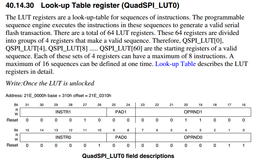
Each Command sequence comprises of one or more 16-bit instructions. Some instructions are followed by an operand, which is usually an address.
Each 16-bit instruction is coded as follows:
msb|15 10|9 8|7 0|lsb
|. . . . . .|. .|. . . . . . . .|
| OpCode | P | Cmd |
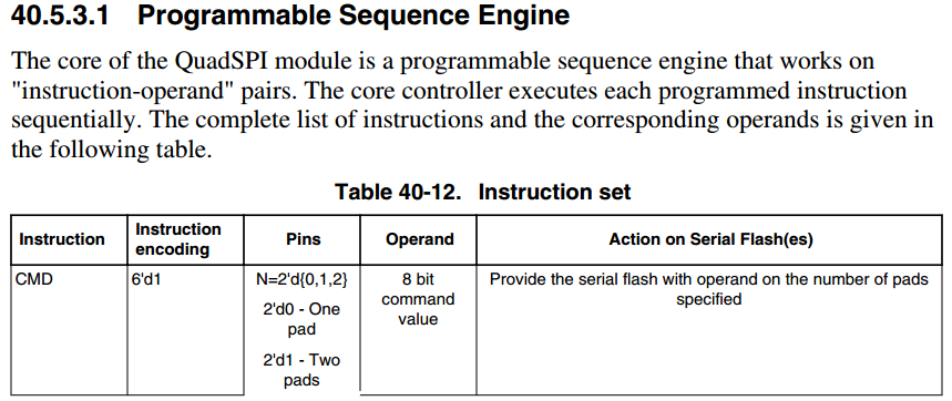
Where Opcode (6-bits [15:10]) is typically:
OPCODE_STOP = 0, //Stop execution and deassert CS
OPCODE_CMD = 1, //Execute command specified in the operand
OPCODE_ADDR = 2, //Provide address cycles for 'operand' number of bits
OPCODE_DUMMY = 3, //Provide the number of dummy cycles in the operand
OPCODE_MODE = 4, //Send flash-specific mode specified in 8-bit operand
OPCODE_MODE2 = 5, //Send flash-specific mode specified in 2-bit operand
OPCODE_MODE4 = 6, //Send flash-specific mode specified in 4-bit operand
OPCODE_READ = 7, //Receive from flash device the number of bytes in the operand
OPCODE_WRITE = 8, //Send to flash device the number of bytes in the operand
OPCODE_JMP_ON_CS = 9, //Jump to instruction index in the operand, if CS is deasserted
OPCODE_ADDR_DDR = 10, //Same as OPCODE_ADDR, but transmit at each clock edge
OPCODE_MODE_DDR = 11, //Same as OPCODE_MODE, but transmit at each clock edge
OPCODE_MODE2_DDR = 12, //Same as OPCODE_MODE2, but transmit at each clock edge
OPCODE_MODE4_DDR = 13, //Same as OPCODE_MODE4, but transmit at each clock edge
OPCODE_READ_DDR = 14, //Same as OPCODE_READ, but transmit at each clock edge
OPCODE_WRITE_DDR = 15, //Same as OPCODE_WRITE, but transmit at each clock edge
OPCODE_DATA_LEARN = 16, //Learn correct DDR sampling point using the given number of data bytes
OPCODE_CMD_DDR = 17, //Same as OPCODE_CMD, but transmit at each clock edge
OPCODE_CADDR = 18, //Provide column address cycles for 'operand' number of bits
OPCODE_CADDR_DDR = 19, //Same as OPCODE_CADDR, but transmit at each clock edge
Where P (2 bits [9:8]) is the number of data pins for data transfer. Values:
DATAPINS_1 = 0, // Use 1 pin
DATAPINS_2 = 1, // Use 2 pins,
DATAPINS_4 = 2, // Use 4 pins
DATAPINS_8 = 3, // Use 8 pins,
Where Cmd - 8 bits [7:0] - NOR Flash Command as per the product Datasheet.
We have known how to write one sequence for a new QSPI flash。
The sequence is just for READ or FAST READ command,system can boot up from QSPI flash。
But there are 64 sequences,is the first sequence only for READ or NOT?
We don't know how to set the other sequence(e.g. Read Status, Erase Sector,Page Program)
Can we put these sequence anywhere in LUT?
If yes,How does imx6ul know what order I put in LUT?
If no,could you give us the order?
Thank you!
Dear
your question is already sloved ? I have the same question with you.
Hi junix
one can check sect.40.5.3.4 Look-up Table i.MX6UL Reference Manual
http://cache.freescale.com/files/32bit/doc/ref_manual/IMX6ULRM.pdf
and mfg tools (link below) qspi-header scripts
i.MX 6 / i.MX 7 Series Software and Development Tool|NXP
Best regards
igor
-----------------------------------------------------------------------------------------------------------------------
Note: If this post answers your question, please click the Correct Answer button. Thank you!
-----------------------------------------------------------------------------------------------------------------------
Hi Igor,
I found 3 config files for 3 NOR flash under MFG tool files。
qspi-nor-macronix-mx25l51245g-config
qspi-nor-micron-n25q256a-config
qspi-nor-spansion-s25fl128s-config
We need to make qspi-nor-winbond-w25q128fv-config .Mainly to modify the LUT part。
n25q256a LUT
2818043d /*lut[0] command sequence*/
39040d06 /*lut[1] command sequence*/
2400 /*lut[2] command sequence*/
0 /*lut[3] command sequence*/
mx25l51245g LUT
0818040B /*lut[0] command sequence*/
1C040C08 /*lut[1] command sequence*/
00002400 /*lut[2] command sequence*/
0 /*lut[3] command sequence*/
s25fl128s LUT
2a1804ed /*lut[0] command sequence*/
0e082e01 /*lut[1] command sequence*/
24003a04 /*lut[2] command sequence*/
0 /*lut[3] command sequence*/
These squence is Great difference and there is no law to follow except command words。
I am very confused about the bold font bytes。
Could you help me to explain the meaning of these bytes?
thanks!
Best Regards,
Junix Wu
Hi Junix
I think you are right, there is no law and these are parts from
different vendors, so you need carefully read W25Q128FV
datasheet and create for it necessary data.
Best regards
igor
Hi Igor,
thank you first of all!
I've read these documents many times.
one can check sect.40.5.3.4 Look-up Table i.MX6UL Reference Manual
http://cache.freescale.com/files/32bit/doc/ref_manual/IMX6ULRM.pdf
and mfg tools (link below) qspi-header scripts
i.MX 6 / i.MX 7 Series Software and Development Tool|NXP
I modified the script(ucl2.xml) of MFG tool to read out the header content.
<CMD state="Updater" type="push" body="$ sh qspi-header.sh $FILE"> Generating the ascii value header</CMD>
<!--hexdump to convert ascii value to hex file-->
<CMD state="Updater" type="push" body="$ cat qspi-tmp">print qspi-tmp (added by wujun)</CMD>
<CMD state="Updater" type="push" body="$ busybox hexdump -R qspi-tmp > qspi-header">Converting ascii value to hex file</CMD>
we can see that:
UTP: executing "sh qspi-header.sh $FILE"
UTP: sending Success to kernel for command $ sh qspi-header.sh $FILE.
utp_poll: pass returned.
UTP: received command '$ cat qspi-tmp'
UTP: executing "cat qspi-tmp"
00000000 00 00 00 00 00 00 00 00 00 00 00 00 00 00 00 00
00000010 00 00 00 00 00 00 00 00 00 00 00 00 00 00 00 02
00000020 03 00 00 00 03 00 00 00 00 00 00 08 00 00 00 00
00000030 00 00 00 08 00 00 00 00 00 00 00 00 00 00 00 00
00000040 02 00 00 00 00 00 00 00 01 00 00 00 00 00 00 00
00000050 00 00 00 00 00 00 00 00 00 00 00 00 00 00 00 00
00000060 00 00 00 00 00 00 00 00 3d 04 18 28 06 0d 04 39
00000070 00 24 00 00 00 00 00 00 00 00 00 00 00 00 00 00
00000080 00 00 00 00 00 00 00 00 00 00 00 00 00 00 00 00
I think this header is specially designed for N25Q256A
Is this header suitable for W25Q128FV?
If not, how do we understand the meaning of these bytes "3d 04 18 28 06 0d 04 39".
3dh is DUAL OUTPUT FAST READ command which I can find in the datasheet of N25Q256A.
what about 04h, 28h, 0dh and 39h?
This problem is very urgent. Please help,THANK YOU!
Hi All,
I am also facing the same issue, is it resolved? if so can you please share the u-boot image so that I can test with uuu tool on my custom board with iMX6Q.
Thanks in Advance
Satish


