- Forums
- Product Forums
- General Purpose MicrocontrollersGeneral Purpose Microcontrollers
- i.MX Forumsi.MX Forums
- QorIQ Processing PlatformsQorIQ Processing Platforms
- Identification and SecurityIdentification and Security
- Power ManagementPower Management
- Wireless ConnectivityWireless Connectivity
- RFID / NFCRFID / NFC
- MCX Microcontrollers
- S32G
- S32K
- S32V
- MPC5xxx
- Other NXP Products
- S12 / MagniV Microcontrollers
- Powertrain and Electrification Analog Drivers
- Sensors
- Vybrid Processors
- Digital Signal Controllers
- 8-bit Microcontrollers
- ColdFire/68K Microcontrollers and Processors
- PowerQUICC Processors
- OSBDM and TBDML
- S32M
-
- Solution Forums
- Software Forums
- MCUXpresso Software and ToolsMCUXpresso Software and Tools
- CodeWarriorCodeWarrior
- MQX Software SolutionsMQX Software Solutions
- Model-Based Design Toolbox (MBDT)Model-Based Design Toolbox (MBDT)
- FreeMASTER
- eIQ Machine Learning Software
- Embedded Software and Tools Clinic
- S32 SDK
- S32 Design Studio
- GUI Guider
- Zephyr Project
- Voice Technology
- Application Software Packs
- Secure Provisioning SDK (SPSDK)
- Processor Expert Software
-
- Topics
- Mobile Robotics - Drones and RoversMobile Robotics - Drones and Rovers
- NXP Training ContentNXP Training Content
- University ProgramsUniversity Programs
- Rapid IoT
- NXP Designs
- SafeAssure-Community
- OSS Security & Maintenance
- Using Our Community
-
- Cloud Lab Forums
-
- Knowledge Bases
- ARM Microcontrollers
- i.MX Processors
- Identification and Security
- Model-Based Design Toolbox (MBDT)
- QorIQ Processing Platforms
- S32 Automotive Processing Platform
- Wireless Connectivity
- CodeWarrior
- MCUXpresso Suite of Software and Tools
- MQX Software Solutions
- RFID / NFC
-
- Home
- :
- Wireless Connectivity
- :
- Wireless MCU
- :
- PN7160调试疑问请教
PN7160调试疑问请教
- Subscribe to RSS Feed
- Mark Topic as New
- Mark Topic as Read
- Float this Topic for Current User
- Bookmark
- Subscribe
- Mute
- Printer Friendly Page
PN7160调试疑问请教
- Mark as New
- Bookmark
- Subscribe
- Mute
- Subscribe to RSS Feed
- Permalink
- Report Inappropriate Content
各位前辈、道友好,小弟使用PN7160设计实现NFC的读卡功能,目前调试发现VBAT、VDD(UP)和VDD(PAD)采用3.3V供电,10PCS有1PCS出现读卡异常,现象为读不到卡,用示波器挂测电源也是稳定没有掉电或者回沟低于标称的Vmin(2.8V),然后把整体的输入电压抬高到4.0V就可以正常读到卡,不太明白其中的原因,我原本的猜想是供电能量不够RF端的发射,但是示波器挂测又看不到电压跌落,请各位大神指点迷津,谢谢~
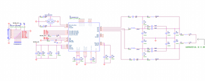
下面附上原理图
- Mark as New
- Bookmark
- Subscribe
- Mute
- Subscribe to RSS Feed
- Permalink
- Report Inappropriate Content
Hello @sheldor0321
After checked your schematic and two suggestions for your reference:
1. Vbat is the main power supply of the NFCC, Vdd(PAD) is the power supply for the host interface and GPIOs. Vdd(UP) is the power supply allowing to generate TXLDO. Their typical operating voltages are different. So, Vbat and Vdd(UP) could be connected to 3.3V, and then it would be better to power Vdd(PAD) separately.
2. For the anormal board on your side, it is recommended that you do a comparison test between normal and abnormal to determine whether VDD(TX) pin is within the normal operating voltage range. The voltage level on TX output buffer is coming from VDD(TX) and this pin is powered internally by the PN7160 thanks to the TXLDO block. The output voltage of this TXLDO can be set between 2.7 V to 5.25 V depending on the VDD(UP) voltage.
Hope the above reply can help you!
Best Regards,
kelly
- Mark as New
- Bookmark
- Subscribe
- Mute
- Subscribe to RSS Feed
- Permalink
- Report Inappropriate Content
Hello kelly,
Thanks for your reply!I have done comparison test between normal boards and abnormal boards,on the normal board VDD(TX) pin is within the normal operaing voltage range,but on the abnormal board VDD(TX) pin is no voltage output.My doubt is that VDD(UP) connected to 3.3V,why do some boards work and some don't work.Then I raised VDD(UP) voltage to 4.0V,the abnormal board works properly.Can you tell me the reason for this problem.
Best regards!
- Mark as New
- Bookmark
- Subscribe
- Mute
- Subscribe to RSS Feed
- Permalink
- Report Inappropriate Content
Hello @sheldor0321
Vdd(PAD) is the power supply for the host interface and GPIOs. I think there may be inconsistencies in the default state of the chip that cause some GPIOs to leak electricity, which leads to some boards abnormal. So, two suggestions for you:
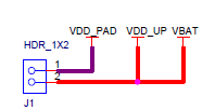
1. Vdd(PAD) Vdd(UP) and Vbat are powered separately, like the following would be better:
2. Initialize all Gpios and the perpherals by software, make sure that the initial state of all boards is consistent.
You can try the above action to see if it works.
Best Regards,
kelly


