- Forums
- Product Forums
- General Purpose MicrocontrollersGeneral Purpose Microcontrollers
- i.MX Forumsi.MX Forums
- QorIQ Processing PlatformsQorIQ Processing Platforms
- Identification and SecurityIdentification and Security
- Power ManagementPower Management
- Wireless ConnectivityWireless Connectivity
- RFID / NFCRFID / NFC
- Advanced AnalogAdvanced Analog
- MCX Microcontrollers
- S32G
- S32K
- S32V
- MPC5xxx
- Other NXP Products
- S12 / MagniV Microcontrollers
- Powertrain and Electrification Analog Drivers
- Sensors
- Vybrid Processors
- Digital Signal Controllers
- 8-bit Microcontrollers
- ColdFire/68K Microcontrollers and Processors
- PowerQUICC Processors
- OSBDM and TBDML
- S32M
- S32Z/E
-
- Solution Forums
- Software Forums
- MCUXpresso Software and ToolsMCUXpresso Software and Tools
- CodeWarriorCodeWarrior
- MQX Software SolutionsMQX Software Solutions
- Model-Based Design Toolbox (MBDT)Model-Based Design Toolbox (MBDT)
- FreeMASTER
- eIQ Machine Learning Software
- Embedded Software and Tools Clinic
- S32 SDK
- S32 Design Studio
- GUI Guider
- Zephyr Project
- Voice Technology
- Application Software Packs
- Secure Provisioning SDK (SPSDK)
- Processor Expert Software
- Generative AI & LLMs
-
- Topics
- Mobile Robotics - Drones and RoversMobile Robotics - Drones and Rovers
- NXP Training ContentNXP Training Content
- University ProgramsUniversity Programs
- Rapid IoT
- NXP Designs
- SafeAssure-Community
- OSS Security & Maintenance
- Using Our Community
-
- Cloud Lab Forums
-
- Knowledge Bases
- ARM Microcontrollers
- i.MX Processors
- Identification and Security
- Model-Based Design Toolbox (MBDT)
- QorIQ Processing Platforms
- S32 Automotive Processing Platform
- Wireless Connectivity
- CodeWarrior
- MCUXpresso Suite of Software and Tools
- MQX Software Solutions
- RFID / NFC
- Advanced Analog
-
- NXP Tech Blogs
- Home
- :
- Software Forums
- :
- S32 SDK
- :
- 3-Wire SPI Configuration SDK
3-Wire SPI Configuration SDK
- Subscribe to RSS Feed
- Mark Topic as New
- Mark Topic as Read
- Float this Topic for Current User
- Bookmark
- Subscribe
- Mute
- Printer Friendly Page
3-Wire SPI Configuration SDK
- Mark as New
- Bookmark
- Subscribe
- Mute
- Subscribe to RSS Feed
- Permalink
- Report Inappropriate Content
Dear Community,
"The functions implemented at the SDK for LPSPI do not have "native support" for 3-wire. So it required to make some changes to support half duplex mode." according to this sentence I have changed to support half duplex mode. I changed to support half duplex mode these functions LPSPI_DRV_MasterInit(..), LPSPI_SetPinConfigMode(..) according to reference manual.
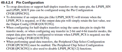
Below is the only information I found in the reference manual about tristate SPI.
According to this information my CFGR1 value is Hex:0x6000001.
lpspi_pin_config_t pinCfg is = LPSPI_SDO_IN_OUT.
lpspi_data_out_config_t dataOutConfig = LPSPI_DATA_OUT_TRISTATE.
bool pcs3and2Enable = true.
Please confirm that configuration and CFGR1 value.
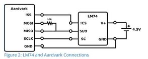
Secondly is there any require HW modification like depicted in the below.
Our schematic design does not have a 10K resistor between MOSI and MISO; instead, it has a 0-ohm resistor. MUST there be a 10K or 1K resistor? Please confirm schematic design.
NOTE: I use S32SDK_S32K1xx_RTM_3.0.0 and S32 Design Studio v2.2
Also I know
"Included on the RTDs comes an example of SPI half duplex transfer. I suggest you take a look at this software supported by S32DS v3.4.Real-Time Drivers for S32K1"
- Mark as New
- Bookmark
- Subscribe
- Mute
- Subscribe to RSS Feed
- Permalink
- Report Inappropriate Content
Hi @maximillion
I answered you in this post
- Mark as New
- Bookmark
- Subscribe
- Mute
- Subscribe to RSS Feed
- Permalink
- Report Inappropriate Content
Hi @VaneB
Secondly is there any require HW modification like depicted in the below.
Isn't the CFGR1 value the same in all 3-wire SPI configurations? So can you confirm that value?
Thanks for answering my those questions.
- Mark as New
- Bookmark
- Subscribe
- Mute
- Subscribe to RSS Feed
- Permalink
- Report Inappropriate Content
Hi @maximillion
The S32K1 does not need to have HW modification, if you configure MOSI as input and output you don have to use any pin for the MISO signal in the PORT module. Also for the other device, the connections depend on its specifications.
Regarding the Configuration Register 1 (CFGR1) value, PINCFG configures SOUT as input and output data, OUTCFG configures the output data as tristated when chip select is negated and PCSCFG configures PCS[3:2] for chip select function. For 3-wire SPI CFGR1 = 0x6000001 is correct, the other bits depend on your application.
- Mark as New
- Bookmark
- Subscribe
- Mute
- Subscribe to RSS Feed
- Permalink
- Report Inappropriate Content
Hi @VaneB
I'm still confused about TXMSK.
Let me explain my LPSPI0 configuration.
1- I use DMA for SPI configuration and I did not set any RX DMA channel because would transmit and receive data at same channel. I set only TX DMA channel. PS continuous is not selected and and bits/frame value is 9.
So TX DMA channel should receive and transmit data. In that case according to your mention TXMSK should be set. I set TXMSK at the LPSPI_DRV_MasterStartTransfer function. Is this correct?
But when I called LPSPI_DRV_MasterGetTransferStatus it return STATUS_BUSY. This value has not changed any time.
Do you have any advice about this topic?

