- Forums
- Product Forums
- General Purpose MicrocontrollersGeneral Purpose Microcontrollers
- i.MX Forumsi.MX Forums
- QorIQ Processing PlatformsQorIQ Processing Platforms
- Identification and SecurityIdentification and Security
- Power ManagementPower Management
- Wireless ConnectivityWireless Connectivity
- RFID / NFCRFID / NFC
- MCX Microcontrollers
- S32G
- S32K
- S32V
- MPC5xxx
- Other NXP Products
- S12 / MagniV Microcontrollers
- Powertrain and Electrification Analog Drivers
- Sensors
- Vybrid Processors
- Digital Signal Controllers
- 8-bit Microcontrollers
- ColdFire/68K Microcontrollers and Processors
- PowerQUICC Processors
- OSBDM and TBDML
- S32M
-
- Solution Forums
- Software Forums
- MCUXpresso Software and ToolsMCUXpresso Software and Tools
- CodeWarriorCodeWarrior
- MQX Software SolutionsMQX Software Solutions
- Model-Based Design Toolbox (MBDT)Model-Based Design Toolbox (MBDT)
- FreeMASTER
- eIQ Machine Learning Software
- Embedded Software and Tools Clinic
- S32 SDK
- S32 Design Studio
- GUI Guider
- Zephyr Project
- Voice Technology
- Application Software Packs
- Secure Provisioning SDK (SPSDK)
- Processor Expert Software
-
- Topics
- Mobile Robotics - Drones and RoversMobile Robotics - Drones and Rovers
- NXP Training ContentNXP Training Content
- University ProgramsUniversity Programs
- Rapid IoT
- NXP Designs
- SafeAssure-Community
- OSS Security & Maintenance
- Using Our Community
-
- Cloud Lab Forums
-
- Knowledge Bases
- ARM Microcontrollers
- i.MX Processors
- Identification and Security
- Model-Based Design Toolbox (MBDT)
- QorIQ Processing Platforms
- S32 Automotive Processing Platform
- Wireless Connectivity
- CodeWarrior
- MCUXpresso Suite of Software and Tools
- MQX Software Solutions
- RFID / NFC
-
- Home
- :
- 产品论坛
- :
- S12 / MagniV微控制器
- :
- Regarding dead time insertion in complimentary mode for S12ZVM
Regarding dead time insertion in complimentary mode for S12ZVM
Regarding dead time insertion in complimentary mode for S12ZVM
Dear Team,
Thanks for your continuous support.
I am using edge aligned complimentary mode in SW. Below are my queries,
1. When PWM is applied to Phase A then at first LS will be ON or OFF? What will be the behaviour of HS and LS?
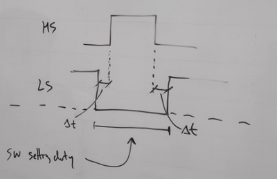
2. Second query is explained though below image, considering as LS will be off first when PWM is applied to phase A.
As per the above image. Our understanding is that "after LS off, HS will be ON after delta t deadtime and after HS off, LS will be on after delta t deadtime. Deadtime will be added on both ends."
Please confirm the understanding is correct or not.
Hello Pratibhasurabhi,
Ad 1)
When you use the standard half-bridge driver for MOSFETs power stage, it uses the boost capacitor to supply high side driver. So the first must be activated low side MOSFET.
The association of complementary channels is in Table 15-18. This means the main channels are Ch_0, Ch_2 and Ch_4.
All depends on the used driver (let use the a standard type – log1 on LS_IN activates the low side MOSFET) then the PWM period must start with PWM_L = 1 and PWM_H = 0 (MCU outputs). This means in complementary mode the PWM output is negated –> PWM_H starts with log0 and channel value = 1-DUTY.
Then for small DUTY the most of period is PWM_H = 0 and PWM_L = 1. The PWM period starts with PWM_H = 0 and PWM_L = 1 – this fits to the standard half-bridge MOSFET driver.
Ad 2)
Please see in Figure 15-41 the detail signal paths. The dead time is inserted always on starting positive output (to delay switch-on of MOSFET) no matter if high-side or low-side – Figure 15-51. Please refer to Figure 1-10 also.
I thing it could help you to solve your task.
Best Regards,
Stano.
