Hi,
I'm using S12ZVML for 24V motor control application by using PMF, internal ADC and external driver.
It is a 15kw fan controller for truck with phase current from -125A~125A with full ADC scale.
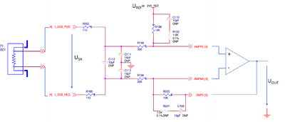
I just refer to the MCSXSR1CS12ZVMUG design guideline with the ADC current sensing circuit, as below and C112 setting 100pF with other components the same .
The current sensing for low current is good,However for high current,like 60Apeak.The driver will trigger the overcurrent protection,for current is not sampling good enough.
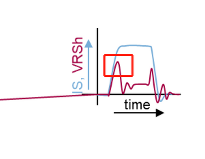
I measure the ADC output pin of AMP0 with high current situation.There is a hurge voltage spike to almost 5.0V and it will keep a long time than decrease.It looks as the below picture shows. I measure the VDDA and 2.5V reference voltage. They both have a ring or oscillation when MOS swithing on/off.
Sine the gain of OP setting is 20. A 0.2V spike will get 4Volt, plus the 2.5V,the OP will go to the saturate situation to 5.0V.
Is it caused by the parasitic effect, and is there any suggestion for me to reduce the effect?
Regards
Arrow
已解决! 转到解答。
Hi,
I hope you are progressing well with your project. In case you would appreciate some shared experience, I would recommend to review the PCB design first. Based on our development, the PCB and routing of the traces is very critical. In our latest EVB https://www.nxp.com/design/development-boards/automotive-motor-control-solutions/magniv-and-s12-solu... we used 400u power traces to eliminate their area and parasitic effects (it is 70 A(RMS) per phase, up to 1kW). In case you can place (+) and (-) power traces on top of each other, you can further decrease the overall parasitic inductance and also significantly improve EMI. Further improvement can be achieved to hide the power traces in the inner two layers of 4-layer PCB, even though the power dissipation solution would be higher. All the steps above have helped in real projects.
Another issue might be linked with the shunt resistor itself. We tried standard flat shunts, but their parasitic inductance (especially if there is a calibration cut) is significant and contributes in high voltage peaks especially in DC-link shunt placement (due to very high di/dt). In the MCSXSR1CS12ZVM, we ended up with a "C"-shaped shunts (see the documentation to this board). The shunt shall be connected using Kelvin connection, with the signal traces of the same length and possibly as short as possible and also perpendicular to the power traces.
We also recommend to have all the analog circuits on a single PCB - in case of integrated solutions, obviously it is the best solution to have S12ZVM on the same board as the power bridge (lead-frame or "sandwich" arrangement is not recommended)
Finally some hidden connection between the DC-link shunt resistor performance and MOSFET switching - in case there is some ringing on the shunt itself, the entire power bridge is floating with this ringing against ground, which might impact the MOSFET switching performance and create additional voltage peaks on motor phases or even on the DC link (+).
I hope it helps at least a little.
Best regards,
Matej
I think it is not 15kW, but 1.5kW fan controller. Then the ADC range has to be set-up to +-125A max peak current.
I suppose the sense resistor is 1mOhm, then max peak current of 125A => 125mV and with Ga = 20 the amp output = 2.5V + 2.5Vref = 5V. So there is no such margin area. It could be good to decrease the Gamp to lower value e.g. 18.
The next very important aspect is the PCB layout design and position of critical components to each other. The parasitic inductance can very simply cause resonant peaks on measured signal and consecutive fault events.
The scope probe connection during measurement is important also. The good option is to use the spring pin on GND instead of standard short wire with clips and isolated grounds between application and scope. In that case you can simply measure non-ground referenced signals also.
When you have measured right signals you can find the place where the issue arise. It is mostly on not proper PCB design or components positions.
The next solution could be use the current sense IC which has isolated internal current sense resistor (usually 0.1 – 0.2 mOhm) and also possible filtered output signal. Then the high current part of design can be isolated from sensitive current sense circuitry and the PCB layout influence can be mostly eliminated.
Please see the attached Guidelines for the external component selection also.
I wish you success in solve this issue.
Yes.
It's my mistake.It's 1.5KW fan controller with rated phase current of 90Apeak.
The shunt is 1mOhm. Because the heat of MOSFET, the logical control part and power part are separated.
The MOS and shunt are on the other metal board. There are some distance for high and low leg MOS.
So it is challenging to reduce the parasitic side effect. Also the VDS has a more spike with 20V on high load.
I'll do more test to check if there is any progress, by decreasing the driving crrent to slow down the switching speed, also the RC snubber.
By the way, the external driver has a dead time of at least 500ns. Do I need to do some care for the software,except the sampling window size? For the dead time ,the voltage forced on the motor will be less than the wanted value.
Regards
Arrow
Hi,
I hope you are progressing well with your project. In case you would appreciate some shared experience, I would recommend to review the PCB design first. Based on our development, the PCB and routing of the traces is very critical. In our latest EVB https://www.nxp.com/design/development-boards/automotive-motor-control-solutions/magniv-and-s12-solu... we used 400u power traces to eliminate their area and parasitic effects (it is 70 A(RMS) per phase, up to 1kW). In case you can place (+) and (-) power traces on top of each other, you can further decrease the overall parasitic inductance and also significantly improve EMI. Further improvement can be achieved to hide the power traces in the inner two layers of 4-layer PCB, even though the power dissipation solution would be higher. All the steps above have helped in real projects.
Another issue might be linked with the shunt resistor itself. We tried standard flat shunts, but their parasitic inductance (especially if there is a calibration cut) is significant and contributes in high voltage peaks especially in DC-link shunt placement (due to very high di/dt). In the MCSXSR1CS12ZVM, we ended up with a "C"-shaped shunts (see the documentation to this board). The shunt shall be connected using Kelvin connection, with the signal traces of the same length and possibly as short as possible and also perpendicular to the power traces.
We also recommend to have all the analog circuits on a single PCB - in case of integrated solutions, obviously it is the best solution to have S12ZVM on the same board as the power bridge (lead-frame or "sandwich" arrangement is not recommended)
Finally some hidden connection between the DC-link shunt resistor performance and MOSFET switching - in case there is some ringing on the shunt itself, the entire power bridge is floating with this ringing against ground, which might impact the MOSFET switching performance and create additional voltage peaks on motor phases or even on the DC link (+).
I hope it helps at least a little.
Best regards,
Matej
Thanks for more details about your solution.
I think the main issue is the design on several boards / parts. Then the parasitic inductance is very high.
The power loss on current sense resistor is about 10W for 100A – it is very high. So I suggest you to use current sense IC e.g. ACS772 with internal sensor of 100uOhm. All current sensors must be integrated on one board very close to power MOSFETs – the parasitic inductance must be eliminated as much as possible. The MOSFET drivers must be placed as close to the MOSFETs as possible too. It eliminates the parasitic inductance in the gate-source circuit – it is important for proper control of the MOSFETs.
Finally you will have two boards – power and control. You need carefully consider the position of the control board relative to power board. The high currents will produce high intensity electromagnetic field which could generate spikes on the sensitive measurement and control signals.
I suggest you to use four layer PCB and all sensitive signal put on internal layer. All signals from one sensor must be routed close each-other and shielded by non-power GND on top and bottom layer like a coax cable. The GND vias must connect those GND layers to form coax cable too. All these control and measurement signals have to as short as possible also. I know it is challenge but whole design is challenge.
The 500ns dead time of the external driver is OK. If the forced voltage on the motor is low due this dead time use lower switching frequency – sufficient is 20kHz. The switching losses will decrease too.
I think the suggested design topology will help you to solve your issue. I wish you success.
Best Regards
Stano.
Hello Arrow,
I agree with Matej’s comment – the right PCB design is very important for this application because of high currents on PCB. The each even a small parasitic inductance can cause the high voltage peaks and all measurements are degraded.
Please consider the price of the dedicated current sense IC and special “C” type of the current sense resistor. In case you use resistor the soldering quality has big influence to right measurements too.
Best Regards,
Stano.
Hi, Stano&Matej
Thanks for your advice.
We have got some progress with the project, by decreasing the driving current, adding a snuber RC filter between DS of MOSFET, and adjusting the filter circuit for current sensing.
Now it can go to the full load with low speed.(phase current to 90Apeak)
There are still some chanllenge with current sensing.Now we use the second and the forth sampling results to do the clark transform.Since the first and the third results are easily to go to the saturate value.
Btw, the current sensor IC is a little expensive, so it may not be our best choice by tradeoff.What we use is BVS-A-R001-1.0,which has bigger power rating and low inductance(less than 3nH).
I'm going to close this thread, since this problem is almost solved.
There are some other issues we encountered,and I'll put a new thread.
Thanks again for your valuable suggestion.
Arrow

