- NXP Forums
- Product Forums
- General Purpose MicrocontrollersGeneral Purpose Microcontrollers
- i.MX Forumsi.MX Forums
- QorIQ Processing PlatformsQorIQ Processing Platforms
- Identification and SecurityIdentification and Security
- Power ManagementPower Management
- MCX Microcontrollers
- S32G
- S32K
- S32V
- MPC5xxx
- Other NXP Products
- Wireless Connectivity
- S12 / MagniV Microcontrollers
- Powertrain and Electrification Analog Drivers
- Sensors
- Vybrid Processors
- Digital Signal Controllers
- 8-bit Microcontrollers
- ColdFire/68K Microcontrollers and Processors
- PowerQUICC Processors
- OSBDM and TBDML
-
- Solution Forums
- Software Forums
- MCUXpresso Software and ToolsMCUXpresso Software and Tools
- CodeWarriorCodeWarrior
- MQX Software SolutionsMQX Software Solutions
- Model-Based Design Toolbox (MBDT)Model-Based Design Toolbox (MBDT)
- FreeMASTER
- eIQ Machine Learning Software
- Embedded Software and Tools Clinic
- S32 SDK
- S32 Design Studio
- GUI Guider
- Zephyr Project
- Voice Technology
- Application Software Packs
- Secure Provisioning SDK (SPSDK)
- Processor Expert Software
-
- Topics
- Mobile Robotics - Drones and RoversMobile Robotics - Drones and Rovers
- NXP Training ContentNXP Training Content
- University ProgramsUniversity Programs
- Rapid IoT
- NXP Designs
- SafeAssure-Community
- OSS Security & Maintenance
- Using Our Community
-
- Cloud Lab Forums
-
- Home
- :
- QorIQ Processing Platforms
- :
- QorIQ
- :
- Re: LX2160A DDR4 Memory Configuration problem
LX2160A DDR4 Memory Configuration problem
- Subscribe to RSS Feed
- Mark Topic as New
- Mark Topic as Read
- Float this Topic for Current User
- Bookmark
- Subscribe
- Mute
- Printer Friendly Page
LX2160A DDR4 Memory Configuration problem
- Mark as New
- Bookmark
- Subscribe
- Mute
- Subscribe to RSS Feed
- Permalink
- Report Inappropriate Content
Is it possible to set parameters with QCVS and obtain valid values through validation after target connection? I found a different item in QCVS DDR test by selecting a different device than when it was an lx2160a device. why different?
Is there a document that can set parameters of descrete DDR4 in Excel file for lx2160a? (Related parameters are automatically filled in)
What's the best way to get the parameters to make a custom board's Descrte ddr4 work? If you have any related data, please let me know.
Boot log and document about MT40A1G16 are attached. Please tell me the next steps.
Note. the boot log used NODIMM config / 1600MT/s
And We have a one more question.
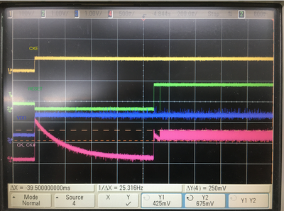
Are the signals below OK?
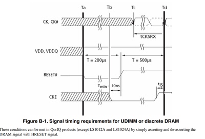
Referring to the documentation of AN5097, the CKE signal should go HIGH after the RESET signal, but it doesn't seem to be the case.
In the case of the same DDR clock, the signal looks small.
Can you give us your opinion?
Thanks,
- Mark as New
- Bookmark
- Subscribe
- Mute
- Subscribe to RSS Feed
- Permalink
- Report Inappropriate Content
Hi @DohwanAhn
Please use CodeWarrior QCVS DDR Tool to configure validate the DDR controller settings.
See the following video:
https://www.nxp.com/video/configure-qoriq-ddr-in-3-minutes:QRIQ-DDR-CONFIGURATION
Thanks
Khushbu
- Mark as New
- Bookmark
- Subscribe
- Mute
- Subscribe to RSS Feed
- Permalink
- Report Inappropriate Content
I've iterated the solution you presented. However, centering the clock just like the video flickers and then passes without any indication. The second video fails to find the vref start value. READ/WRITE ODT also both fail. Booting was done in FLEXSPI boot mode.
Thanks,
- Mark as New
- Bookmark
- Subscribe
- Mute
- Subscribe to RSS Feed
- Permalink
- Report Inappropriate Content
Hi @DohwanAhn
Please configure the Properties panel according to the DDR datasheet.Please make sure that valid RCW configuration is loaded on the board.
Can you please share custom board's schematic so that we can verify it?
Thanks
Khushbu
- Mark as New
- Bookmark
- Subscribe
- Mute
- Subscribe to RSS Feed
- Permalink
- Report Inappropriate Content
We've seen the problem occur through the console debug logs when perform `Centering the clock`. What can I check?
Thanks,
#################### Result for: ddr_vref_searcher ###### Run 1 ###################################
Test result: [
Traceback (most recent call last):
File "C:\Freescale\CW4NET_v2020.06\Common\QCVS\Optimization\resources\QorIQ\ARMv8/ddr/ddr_vref_searcher.py", line 167, in ddr_phy_vref_searcher
if not checkConfiguration(params, session, ddr_ctrl_idx):
File "C:\Freescale\CW4NET_v2020.06\Common\QCVS\Optimization\resources\QorIQ\ARMv8/ddr/ddr_vref_searcher.py", line 68, in checkConfiguration
sys_init.init(params, session, False)
File "C:\Freescale\CW4NET_v2020.06\Common\QCVS\Optimization\resources\QorIQ\ARMv8\ddr\sys_init.py", line 150, in init
reset_out = utils.gdb_execute("cw_reset %d" % reset_delay)
File "C:\Freescale\CW4NET_v2020.06\Common\QCVS\Optimization\resources\QorIQ\ARMv8\common\utils.py", line 215, in gdb_execute
raise gdb.GdbError("ERROR: " + str(ex))
GdbError: ERROR: Target reset failed.
//
Additional error details:
[CCS: timeout during target operation]
- Mark as New
- Bookmark
- Subscribe
- Mute
- Subscribe to RSS Feed
- Permalink
- Report Inappropriate Content
Hi @DohwanAhn
Please make sure:
1) JTAG connection circuit is implemented exactly as shown in the AN5407 - Layerscape LX2160A and LX2162A Design Checklist, Figure 36. JTAG interface connection.
2) Reset to SDRAM devices is implemented as proposed in the AN5097 - Hardware and Layout Design Considerations for DDR4 SDRAM, Appendix B DRAM reset signal considerations.
Please provide a digital scope trace showing behaviour of PORESET_B, HRESET_B and SDRAM reset signals.
Thanks
Khushbu
- Mark as New
- Bookmark
- Subscribe
- Mute
- Subscribe to RSS Feed
- Permalink
- Report Inappropriate Content
We fixed a reset related issue. Then, we successfully performed validation and confirmed that there was no fail. However, I created an expert code and applied it to the source, but ddr does not work normally.
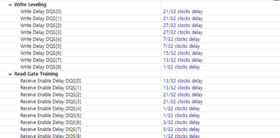
When performing clock validation, we saw that appropriate clock delay values were selected in write leveling and read gate training. What register is this value stored in? We can't see the relevant value in the generated ddr_init.c. For ls1046, wrlvl control register exists - (DDR1_DDR_WRLVL_CNTL/2/3) . However, it does not exist on the lx2160a. If the lx2160a doesn't support it, this test seems meaningless. What should we do? Looking forward to your reply. thank you
- Mark as New
- Bookmark
- Subscribe
- Mute
- Subscribe to RSS Feed
- Permalink
- Report Inappropriate Content
Hi @DohwanAhn
The LX2160 automatically calibrates 'write leveling' and 'clock adjust' parameters for the DDR4 PHY at start up.
"ddr does not work normally".
Can you please share log with log level INFO.
Thanks
Khushbu
- Mark as New
- Bookmark
- Subscribe
- Mute
- Subscribe to RSS Feed
- Permalink
- Report Inappropriate Content


