- Forums
- Product Forums
- General Purpose MicrocontrollersGeneral Purpose Microcontrollers
- i.MX Forumsi.MX Forums
- QorIQ Processing PlatformsQorIQ Processing Platforms
- Identification and SecurityIdentification and Security
- Power ManagementPower Management
- Wireless ConnectivityWireless Connectivity
- RFID / NFCRFID / NFC
- MCX Microcontrollers
- S32G
- S32K
- S32V
- MPC5xxx
- Other NXP Products
- S12 / MagniV Microcontrollers
- Powertrain and Electrification Analog Drivers
- Sensors
- Vybrid Processors
- Digital Signal Controllers
- 8-bit Microcontrollers
- ColdFire/68K Microcontrollers and Processors
- PowerQUICC Processors
- OSBDM and TBDML
- S32M
-
- Solution Forums
- Software Forums
- MCUXpresso Software and ToolsMCUXpresso Software and Tools
- CodeWarriorCodeWarrior
- MQX Software SolutionsMQX Software Solutions
- Model-Based Design Toolbox (MBDT)Model-Based Design Toolbox (MBDT)
- FreeMASTER
- eIQ Machine Learning Software
- Embedded Software and Tools Clinic
- S32 SDK
- S32 Design Studio
- GUI Guider
- Zephyr Project
- Voice Technology
- Application Software Packs
- Secure Provisioning SDK (SPSDK)
- Processor Expert Software
-
- Topics
- Mobile Robotics - Drones and RoversMobile Robotics - Drones and Rovers
- NXP Training ContentNXP Training Content
- University ProgramsUniversity Programs
- Rapid IoT
- NXP Designs
- SafeAssure-Community
- OSS Security & Maintenance
- Using Our Community
-
- Cloud Lab Forums
-
- Knowledge Bases
- ARM Microcontrollers
- i.MX Processors
- Identification and Security
- Model-Based Design Toolbox (MBDT)
- QorIQ Processing Platforms
- S32 Automotive Processing Platform
- Wireless Connectivity
- CodeWarrior
- MCUXpresso Suite of Software and Tools
- MQX Software Solutions
- RFID / NFC
-
- Home
- :
- NXP Tech Blog
- :
- i.MX RT600 Hardware Design – Part 3 of 3 – The RT685 Super-Monkey
i.MX RT600 Hardware Design – Part 3 of 3 – The RT685 Super-Monkey
i.MX RT600 Hardware Design – Part 3 of 3 – The RT685 Super-Monkey
- Subscribe to RSS Feed
- Mark as New
- Mark as Read
- Bookmark
- Subscribe
- Printer Friendly Page
- Report Inappropriate Content
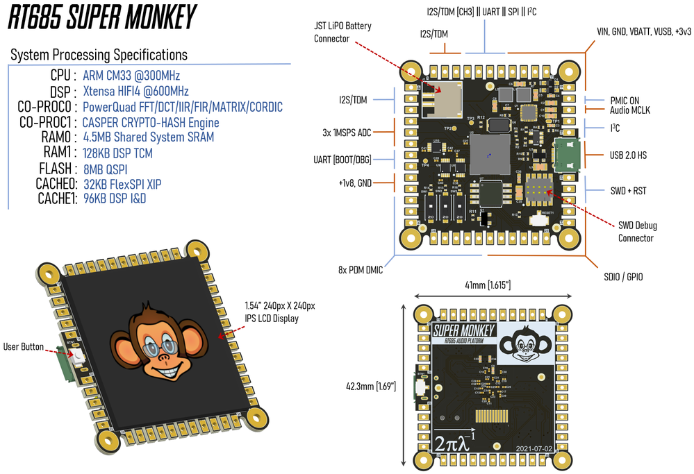
In my previous two articles, we examined the core components to an RT600 hardware design using the code name “Super-Monkey”. The objective of the Super-Monkey project to produce minimal configuration design example using RT685 audio crossover MCU that would support my real-time audio processing projects. There is quite a bit IO available on the RT685, but I chose to constrain my design to the most common functions for real-time audio. My applications generally use professional, “flagship quality” audio codecs for musical instrument signal processing. Using this as a guide, the process of coming up with a minimal IO complement was simplified. It is time to now time reveal the Super-Monkey design!
Figure 1. The RT685 Super-Monkey
I spent quite a bit of time considering a form factor. Since this was my first attempt at an RT600 design, I elected to constrain the formfactor to something known. Last year I developed the
Mini-Monkey around the NXP LPC55S69. For the “Super-Monkey”, I chose to keep this form factor but extend the number of IO. Decision making fatigue is a very real concern for engineers. The “perfect module form factor” trap is easy to fall into. It is tempting to spend a great deal of time optimizing for a general-purpose use case to handle unknown requirements. My experience has shown me that in almost every case, overthinking future possibilities at the outset never pays dividends down the road. We engineer’s love to tinker and will end up making changes anyway. I have two separate projects I want to implement with the RT600 so I decided to focus my efforts exclusively what I need for those efforts. I did receive an excellent suggestion from Greg Steiert to use the SparkFun MicroMod form factor. The MicroMod form factor is compelling Once I verify this design, I will be revisiting this form factor for more general-purpose use cases.
I thought it would be instructive to list some of the high-level processing capabilities available in the RT685 in Figure 1. It is difficult to overstate the amount capability packed into the RT685. Even few years I like to step back and reflect on progress that has been made with MCU integration. It is often too easy to overlook the sum of science & engineering needed to integrate this amount of technology in a 9mmx9mm package. All of it for a few lattes at the coffee shop.
Super-Monkey IO
Power Input
+5v from the micro-USB or IO connector. There is also JST "PH" connector for common LiPO batteries. PCA9420 PMIC has a built in battery charger so the Super-Monkey can be "portable".
Digital Audio IO
The Super-Monkey has two I2S/TDM audio interfaces provided by the flexcomm peripheral. In my applications, I tend to separate the ADC and DAC to achieve the highest SNR. One channel will be used to interface with an 8-channel audio ADC (Cirrus Logic CS5368) and the other will be used with an AES3 Audio Transmitter (Cirrus Logic 8406). The second channel will a drive a professional audio DAC (Cirrus Logic CS4398). For some applications, I prefer audio master clock to be generated with a high-quality, minimal phase noise oscillator. The Super-Monkey has a pin for an audio master clock input that can be used to bring in an external master clock.
Digital Microphones
The Super-Monkey exposes all eight DMIC inputs available on the RT685.
Spare Flexcomm
I reserved pins for one Flexcomm port to be allocated on a per project basis. This will allow me to select I2C, SPI, UART or and extra I2S bus as needed.
Debug UART
There is one dedicated UART exposed via the IO pins. This UART can be used with the ROM bootloader to program flash, fuses, etc.
I3C
I reserved two pins to experiment with the I3C bus. I3C is a new superset of the I2C standard which allows for much faster data rates, multi-master and hot join capability. It lives at an interesting intersection of I2C and SPI so I wanted to platform to run experiments.
SDIO
A 4-bit SDIO port for adding an SD card. I do not have an immediate requirement for SDIO but at a minimum I get a handful of GPIO that are also multiplexed with SCT (State Configuration Timer) channels. I *really* like the SCT in all the LPC families so I made sure to make it available.
ADC
I exposed three inputs to the RT685 1MSPS ADC, two of which can be used to form a fully differntial input. The intent is to use the ADC channels for potentiometers/user input. I have plans for piezo vibration sensor applications as well.
LCD
I borrowed the 1.54” from the LPC55S69 Mini-Monkey Design. In fact, the module form factor was original designed around this specific display. It looks really sharp, so I decided to include it for some neat audio visualizations. It is wired to a dedicate 50MHz high speed SPI port and can achieve high frame rates. Coupled with the large RAM in the RT685, the Super-Monkey can perform some interesting graphics applications.
PCB Routing
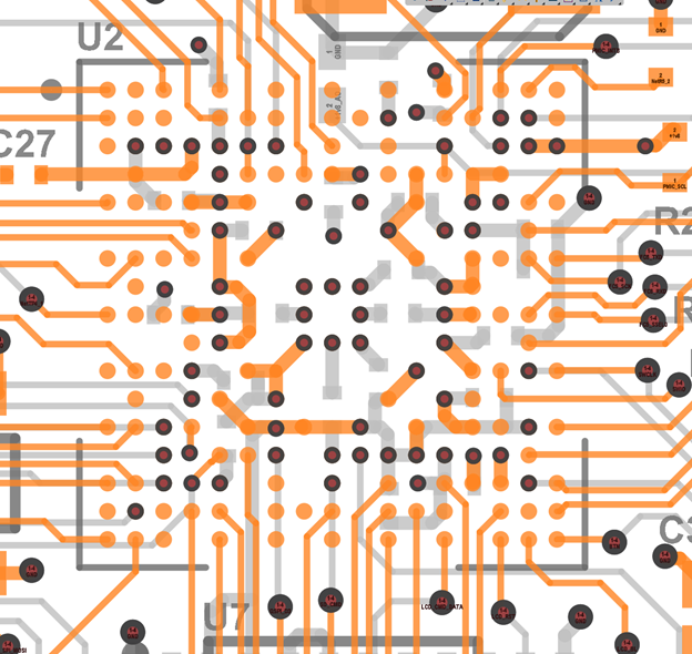
I intended the Super-Monkey to use 4-layer PCB stackup. To achieve a 4-layer design, I had to make some comprises as compared to the layout on RT685-EVK. The RT600 in the VFBGA176 package is straightforward to fan out. In fact, the PCB routing on the RT685-EVK has all IO fanned out on the top layer. One caveat is that 3mil trace/space design rules are required The EVK is quite large and there is plenty of room to bring all the traces on the top layer. The Super-Monkey has more parts placed very close to the MCU package, so I needed to make use of the bottom layer near the package. As an alternative example to the RT685-EVK, I chose to use 5mil design rules coupled with via-in-pad technology to fan out the IO.
Figure 2: Super-Monkey IO Fanout
The via-in-pad geometry used a 12mil pad with 6mil mechanical drill. This geometry is on the edge of where laser microvias would be required. The two inner layers (not shown) are dedicated to return and power (Core, +1.8v and +3.3v). Via-in-pad allowed me to use a more relaxed 5mil trace/space rule which is lower cost and higher yield option as compared to 3mil. Since I did not require all the RT685 IO, keeping to a 4-layer design was straightforward. Via-in-pad does increase cost, but the trade-off vs 3-mil spacing makes it an attractive option to relax the clearance specifications and fanout to other layers. It also allows one place vias on the decoupling pad simplifying placement.
The VFBGA176 package does leave some balls unpopulated making routing and fanout simpler. Most of the core power and ground connectors are on the interior of the package. This alleviates quite a bit of contention with IO. In Figure 2, you can see the 0201 capacitors on the bottom side. I believe with some work, 0402 size capacitors could be used to relax manufacturing tolerances. 0201 capacitors are quite small. Chris Denny of Worthington assembly posted some nice blogs on optimum geometries for high yield when using 0201 packages. He also has a nice article on via-in-pad technology.
It is certainly possible to route the RT685 VFBGA176 on a 4-layer process and still be able to use quite a bit of the IO. In fact, with a bit more work, I feel I could use about 90% of the IO without resorting to use a 6-layer process. While this package is small, it is still possible to use it successfully without breaking the bank with the most expensive PCB process technology.
Wrapping Up
The Super Monkey design is just about ready to send to fab. Once I get to the 99% point, I usually let a design sit for a day or two before I do final inspection, trace clean-up and documentation generation. I find the extra day or day allows my brain to subconsciously think about final steps to get the design over the goal line. Sometimes the extra time can yield additional quality of life improvements in the design.
I will be using CircuitHub for the Super-Monkey prototypes. When the prototypes are ready, I will post a video with the results. Once the design is verified, I’ll make the design files available for anyone to use for bootstrapping a new project. Stayed tuned to the see the RT685 Super-Monkey in *real-life*. While this is the final article in the RT600 hardware design series, I will be posting a few more RT600 related materials including some audio demos. There is more RT600 content coming your way!
Crossing Over With the i.MX RT600 Part 1 of 2
Crossing Over With the i.MX RT600 Part 2 of 2
i.MX RT685 Hardware Design 1 of 3 - Power and Package
i.MX RT685 Hardware Design 2 of 3 - Flash Memory and Boot Configuration
i.MX RT685 Hardware Design 3 of 3 - The SuperMonkey Design
i.MX RT685 SuperMonkey QSPI Bringup with MCUXpresso and Segger J-Link
Creating a Custom Zephyr Board for the i.MX RT685 SuperMonkey
You must be a registered user to add a comment. If you've already registered, sign in. Otherwise, register and sign in.
-
101
6 -
communication standards
4 -
General Purpose Microcontrollers
23 -
i.MX RT Processors
46 -
i.MX Processors
51 -
Interface
1 -
introduction
14 -
LPC Microcontrollers
73 -
MCUXpresso
34 -
MCUXpresso Secure Provisioning Tool
1 -
MCUXpresso Conig Tools
30 -
MCUXpresso IDE
42 -
MCUXpresso SDK
26 -
Model-Based Design Toolbox
6 -
MQX Software Solutions
2 -
QorIQ Processing Platforms
1 -
QorIQ Devices
5 -
S32N Processors
4 -
S32Z|E Processors
6 -
SW | Downloads
8 -
日本語ブログ
6
- « Previous
- Next »

