- Forums
- Product Forums
- General Purpose MicrocontrollersGeneral Purpose Microcontrollers
- i.MX Forumsi.MX Forums
- QorIQ Processing PlatformsQorIQ Processing Platforms
- Identification and SecurityIdentification and Security
- Power ManagementPower Management
- Wireless ConnectivityWireless Connectivity
- RFID / NFCRFID / NFC
- MCX Microcontrollers
- S32G
- S32K
- S32V
- MPC5xxx
- Other NXP Products
- S12 / MagniV Microcontrollers
- Powertrain and Electrification Analog Drivers
- Sensors
- Vybrid Processors
- Digital Signal Controllers
- 8-bit Microcontrollers
- ColdFire/68K Microcontrollers and Processors
- PowerQUICC Processors
- OSBDM and TBDML
- S32M
-
- Solution Forums
- Software Forums
- MCUXpresso Software and ToolsMCUXpresso Software and Tools
- CodeWarriorCodeWarrior
- MQX Software SolutionsMQX Software Solutions
- Model-Based Design Toolbox (MBDT)Model-Based Design Toolbox (MBDT)
- FreeMASTER
- eIQ Machine Learning Software
- Embedded Software and Tools Clinic
- S32 SDK
- S32 Design Studio
- GUI Guider
- Zephyr Project
- Voice Technology
- Application Software Packs
- Secure Provisioning SDK (SPSDK)
- Processor Expert Software
-
- Topics
- Mobile Robotics - Drones and RoversMobile Robotics - Drones and Rovers
- NXP Training ContentNXP Training Content
- University ProgramsUniversity Programs
- Rapid IoT
- NXP Designs
- SafeAssure-Community
- OSS Security & Maintenance
- Using Our Community
-
- Cloud Lab Forums
-
- Knowledge Bases
- ARM Microcontrollers
- i.MX Processors
- Identification and Security
- Model-Based Design Toolbox (MBDT)
- QorIQ Processing Platforms
- S32 Automotive Processing Platform
- Wireless Connectivity
- CodeWarrior
- MCUXpresso Suite of Software and Tools
- MQX Software Solutions
- RFID / NFC
-
- Home
- :
- NXP Tech Blog
- :
- Using the i.MX RT600 Audio EVK as a Digital Audio Engineering Test Bed
Using the i.MX RT600 Audio EVK as a Digital Audio Engineering Test Bed
Using the i.MX RT600 Audio EVK as a Digital Audio Engineering Test Bed
- Subscribe to RSS Feed
- Mark as New
- Mark as Read
- Bookmark
- Subscribe
- Printer Friendly Page
- Report Inappropriate Content
Introduction
One of the most interesting parts in the current MCU landscape is the NXP i.MX RT685 crossover MCU. The i.MX RT685 is a specialized MCU that combines a 300MHz Arm® Cortex® M33 core, a 600MHz Tensilica® HiFi4 DSP, a large amount of internal SRAM (4MB) optimized for multicore access, and plethora of useful general purpose peripherals. This combination of features makes the RT685 well suited to professional audio applications.
The RT685 was initially supported by an EVK, the MIMXRT685-EVK, that exposed all the common features and IO for general purpose development. There is now a special variant of the EVK focus on professional audio applications, the i.MX RT600 Audio Evaluation Kit: i.MX RT685-AUD-EVK.
Figure 1. The i.MX RT600 Audio Evaluation Kit - i.MX RT685-AUD-EVK.
The RT685-AUD-EVK builds on the capabilities of the MIMXRT685-EVK by adding features to support professional audio applications such as
- A Cirrus Logic CS42448 6-Channel 24-bit ADC/DAC
- An expansion port to access all eight digital microphone (DMIC) channels
- An audio expansion port for connecting custom daughter cards.
For this article, I will focus on the audio expansion port and how it can be used to connect alternate audio ADCs and analog front ends. My specific use case for the RT685-AUD-EVK is to construct a development platform for a piezoelectric pickup based guitar. I will be showing how to use the audio daughter card expansion port to connect a specialized, high-performance six-channel ADC along with a charge amplifier front-end that I had been wanting to experiment with.
Using the custom daughter card as a starting point, I will show how to configure the RT685-AUD-EVK to connect the audio daughter card connector and how to leverage an example project in MCUXpresso SDK to quickly get audio streaming into the RT685. Along the way, I will interject some tidbits about high channel count digital audio interfacing, charge amplifiers and guitar signal process that I believe you will find useful.
“Full-Stack” Digital Audio Engineering
Implementing digital audio at the MCU/DSP level is a passion of mine. Specifically, my interest has orbited “real-time” audio processing. This means that algorithms are continuously processed with near zero latency. One such application is real-time processing of musical instruments and vocal effects.
In college, I found there were few courses and resources that connected all the necessary technical pieces to truly enable a “full stack” of digital audio talent. To become an effective digital audio engineer, I had to integrate concepts from analog design, MCUs, PCB layout, Digital Signal Processing (DSP), Electricity and Magnetism, Software Engineering, User Interface Programming, Mechanical Engineering and Systems Engineering.
Integrating small experiences over time was my path to building an effective “stack”. I now try to interject nuggets of information related to the topic wherever I can with the intent that others can find what they may need. I even put together a digital audio engineering special elective at Penn State University for one semester to give Electrical, Computer and Software Engineering students the ability to be introduced to the wide range of information needed to be effective in digital audio engineering.
There are many other disciplines which share common principles so learning “full stack” digital audio engineering can be useful in many other domains including machine condition monitoring, communications, sensor design, machine learning and embedded systems programming. Before we dive into the details of interfacing with the RT685-AUD-EVK, I want to offer some background on my particular project as there may be some pieces you may find relevant to your own efforts.
Piezoelectric Transduction for Musical Instruments
Becoming an effective “full stack” audio engineer means understanding how things work from the physics of sensing mechanism through the electronics design, software to the transducers used to generate sound. Another passion of mine outside of embedded systems engineering is the electric guitar. I am frequently thinking and rethinking of new ways to enhance the instrument.
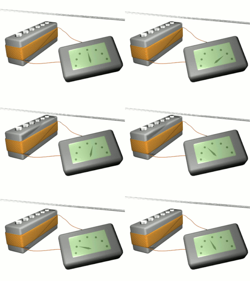
The technology used in most electric guitars is quite simple. The sensing element (the pickup) is effectively an electro-magnetic *velocity* sensor. Pickups are coils of wire wrapped around a relatively weak magnet core.
Figure 2. Single Coil Pickup Construction.
Guitar pickups are placed underneath the strings in various positions along the length of the guitar’s neck. Using the magnetic properties of the metal guitar strings, a pickup translates the acoustic velocity along a small region of the string into an electrical current. The “tone” of the of the pickups is influenced by several factors such as the properties of the magnet, the properties of the coil and the physical position.
Historically speaking, electro-magnetic pickups were the most viable way, both from an engineering and economic perspective, to sense string vibration. There have been advances in material science have enabled alternate methods of sensing acoustic vibrations.
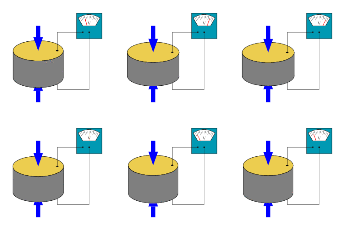
The piezoelectric effect was discovered in 1880 by Jacques and Pierre Curie. Simply put, the piezoelectric effect can be used as transduction mechanism that maps mechanical stress/strain in a physical material to an electric charge.
Figure 3. Piezoelectric Sensors
Many materials exhibit some amount piezoelectric properties in their natural state. This comes as the result of a crystal structure that exhibits a net dipole moment. While some materials exhibit a piezoelectric effect naturally, material scientists and engineers have developed methods to fabricate “smart materials” which optimize/maximize the effect. These “piezoceramics” or “piezos” are found throughout our technological civilization. They can be found in everything from ultrasound probes for medical applications, underwater sonar imaging systems to electronic fuel injectors in vehicles. And as we will soon see, electric guitars!
A while ago, I put together a video explain why piezos were a neat idea for my “guitar active pickguard”.
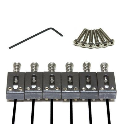
The best way to use a piezo ceramic on the electric guitar is to place the sensor at the bridge. There are commercial products which integrate a piezo ceramic sensor in the bridge saddles to make this easier.
Figure 4. Graphtech Ghost™ Piezoelectric Saddle Pickups.
Mathematically, placement of the of the sensor at the bridge/saddle results in a sensor whose frequency response is not dependent on pickup position. With some DSP algorithms, we can do some interesting things with the guitar tone. In principle, we could replicate almost *any* tone that a coil pickup could generate…. and more!
It is possible to get tones that sound like an acoustic guitar, banjo, steel guitar or mandolin. There are commercial products which use piezo pickups and DSP to do this! With DSP technology, you could even emulate the tone of amplifiers in the guitar itself. The other side effect is that there are individual sensor signals for each string on the guitar. Per string processing enables really neat applications such guitar synthesizers (make a guitar sound like a trombone, flute or violin), real-time accurate pitch shifting (turn a guitar into a bass or doing harmonizing), and dynamic tone shaping that would not be possible with a classic coil pickup.
It is possible to get tones that sound like an acoustic guitar, banjo, steel guitar or mandolin. There are commercial products which use piezo pickups and DSP to do this! With DSP technology, you could even emulate the tone of amplifiers in the guitar itself. The other side effect is that there are individual sensor signals for each string on the guitar. Per string processing enables really neat applications such guitar synthesizers (make a guitar sound like a trombone, flute or violin), real-time accurate pitch shifting (turn a guitar into a bass or doing harmonizing), and dynamic tone shaping that would not be possible with a classic coil pickup.
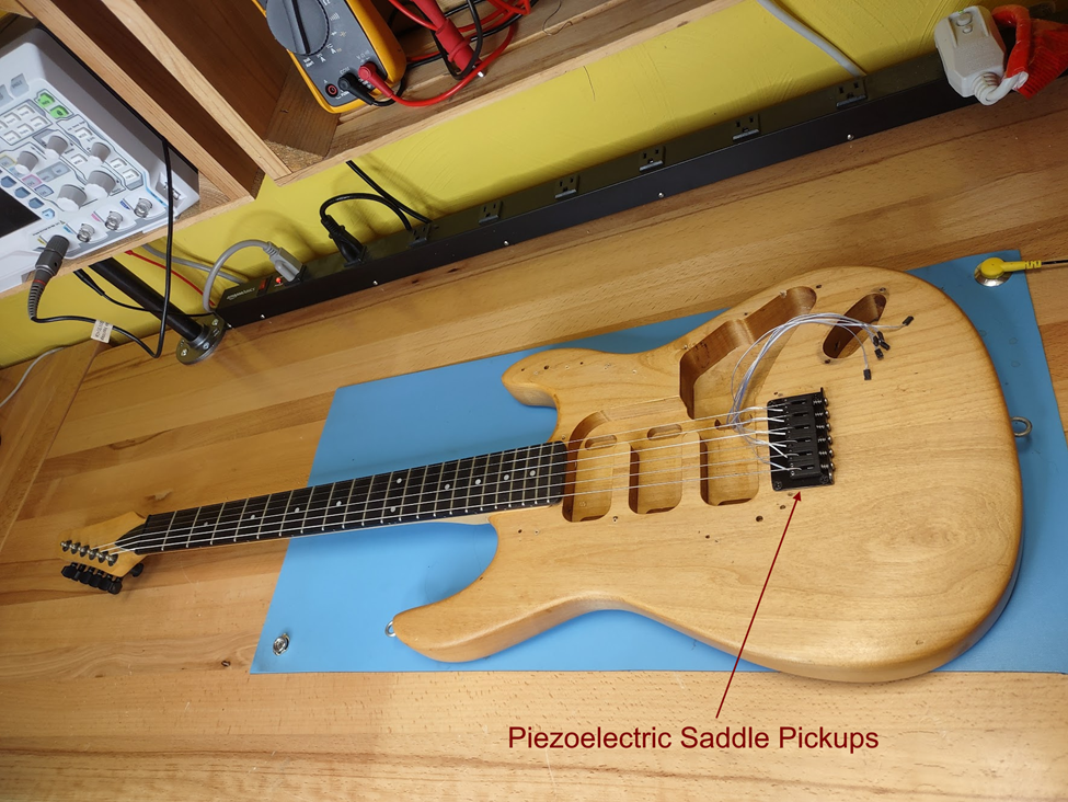
My engineering testing bed guitar is the remnants of a Carvin (now Kiesel Guitars) Bolt-T model which is similar to a Fender® Stratocaster®. I have a set of piezoelectric pickups mounted for experimentation.
Figure 5. Electric Guitar Engineering Test Bed.
Using the daughter card expansion port on the RT685-AUD-EVK, I can have a complete audio development platform to test new algorithms, front end circuitry and experimental features.
The i.MX RT685-AUD-EVK Daughter Card Design
There are pieces of functionality I need on my daughtercard to interface with my piezo pickups:
- Six channels of charge amplifiers
- A Six-Channel analog to digital converter (Cirrus logic CS5366)
An acoustic piezoelectric sensor works by generating a dynamic charge in response to a dynamic stress (think force over some unit area) on the surface of the sensor structure. I am leaving out some of the mathematical details, but this is an effective initial model to understand what is going on. In the low frequency, long wavelength limit, a piezoelectric structure looks effectively like a capacitor at its electrical port. While you may initially think of the sensor output as a “voltage” signal, it is more useful to think of it as a source of electric charge.
To properly interface with the piezoelectric sensor, one must use a charge amplifier. A charge amplifier circuit translates the dynamic charge signal from the piezo into a low output impedance voltage source. There are a couple advantages of charge amplifiers. One being that the gain (in the single ended case) is controlled completely by a feedback capacitor. In some scenarios, the cable capacitance connecting the piezo is significant but does not influence the gain of the amplifier. There is, however, the possibility that the charge will amplify charges resulting from other sources in in the system such as the cable insulation itself!. A good starting point for charge amplifiers is on Wikipedia.
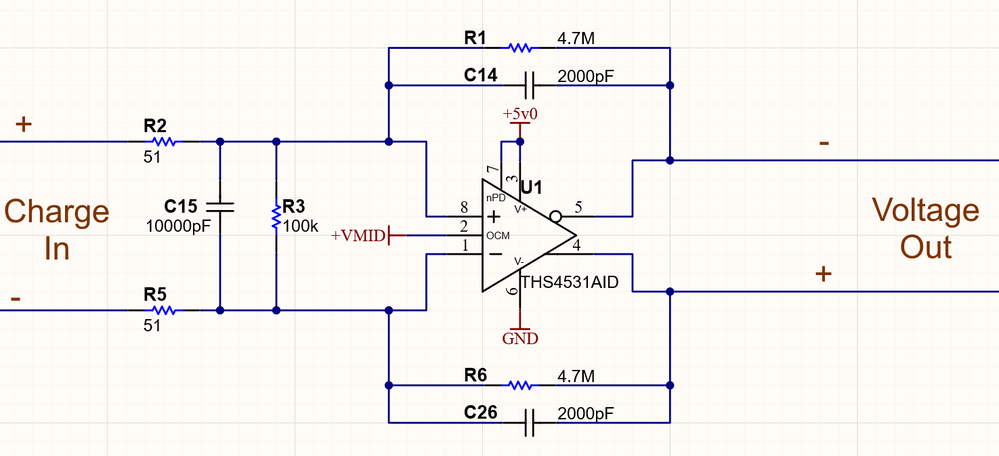
Since a piezo ceramic sensor is a two-terminal electrical device, it can be applied in a fully differential manner. The ADC I selected for the test bed was a Cirrus logic CS5366 which has six fully differential inputs.
The plan for my daughter card was to use a fully differential charge amplifier so the signal transmission can be differential from sensor to the ADC. In the past, I have used a few different charge amplifier configurations using generic op-amps. In this case, I wanted to experiment with a design based upon a THS4531 fully differential amplifier.
The THS4531 is like a common op-amp except that the output is fully differential. It also has a terminal to set a common mode offset which is helpful for connecting directly to a data converter with pseudo differential inputs.
Figure 6. Fully Differential Charge Amplifier.
The THS4531 differential outputs can directly drive the differential inputs of the CS5366.
The reason I chose the CS5366 was two-fold:
- It has best in class dynamic range for a six-channel device at 114db and a -105dB THD+N characteristic. This can be important for algorithms that model guitar tube amplifiers. The CS42448 onboard the RT685-AUD-EVK exhibits a 105db dynamic range and -98dB THD+N.
- The device is an ADC only and can be configured for operation with pull-ups/pull-down at reset. This makes fixed configuration designs simple.
The CS42448 is a highly integrated device that has both six channel of ADC and six channels of DAC. It is typical in very high-performance audio systems for the ADC and DAC to be separate chips to achieve the highest SNR and dynamic range. Since I was interfacing my sensors into the code with a specialized charge amp circuit, I want to use an ADC dedicated to that purpose.
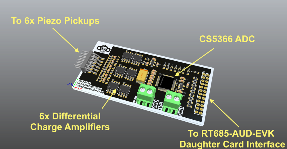
My daughter card design turned out to be compact and easy to build.
Figure 7. Custom RT685-AUD-EVK Daughter Card Design.
Real world pictures are shown at the end of this article. In addition to the core circuitry, I added Phoenix style screw terminals to provide external power for the +5v Analog and Digital sections of the CS5366.The +5v rails from the RT685-AUD-EVK is sourced from the USB bus and I wanted to provide clean power to the analog frontend and the CS5366.
Differential Charge Amp – First Look
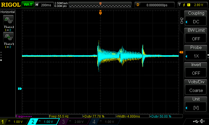
Once I received my prototype PCBs, I was able to do a quick check that the charge amps worked with my piezo pickups. The first test was to check max levels and the bias being fed into the CS5366. Figure 8 shows the charge amplifier output on the “A” string while playing Stevie Ray Vaughan style note stabs. This will generate impulse responses in the pickup that will be close to what I would consider a “maximum input”.
Figure 8. Initial Charge Amplifier Testing – Bias and Level Check.
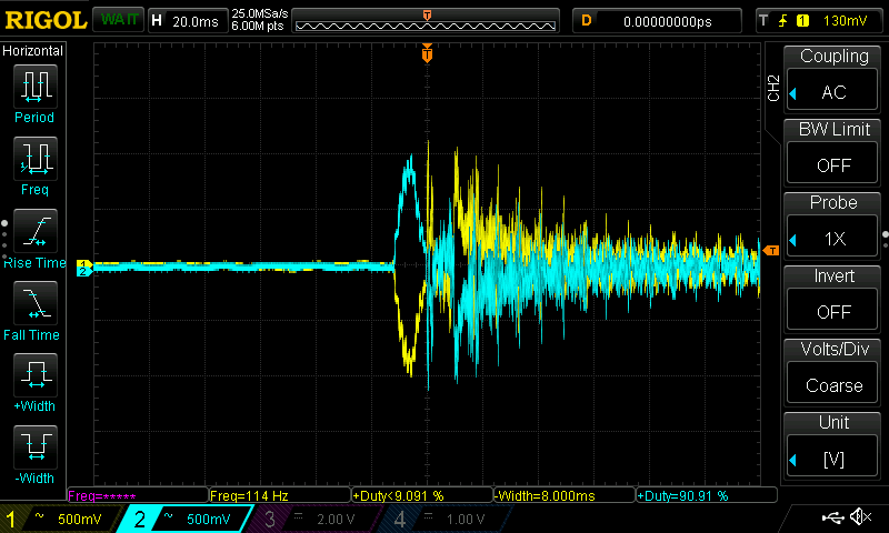
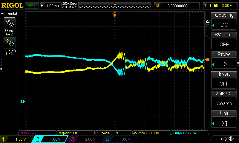
The differential inputs of the CS5366 should be centered around +VQ (nominally +2.5V) and should be within a nominal 5V range. Zooming in on the waveform in figure 8 and enabling AC coupling, we can see the differential behavior.
Figure 9. Charge Amplifier Differential Output Check Level Check.
We can see that the signal is nominally OK in terms of the differential behavior. From here we can fully evaluate noise performance of the sensor through the CS5366. An important note about piezo sensors is that they can produce harmonically rich signals. Even though I was playing on the “A” string, the piezo sensor will provide you with almost everything that is happening on the string. You will not see pure sine waves with the exception of when playing natural harmonics. There is a lot happening on a guitar string and you almost never get a pure sinusoidal tone.
Figure 10. Complex Vibration Signals from the Piezo Pickup.
Interfacing Digital Audio Via the RT685-AUD-EVK Daughter Card Expansion Port
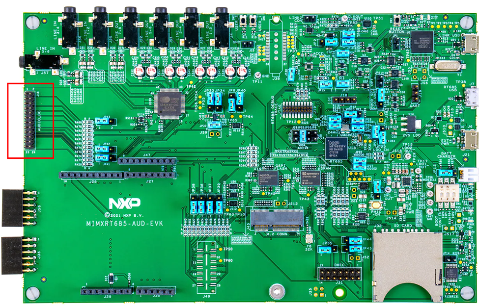
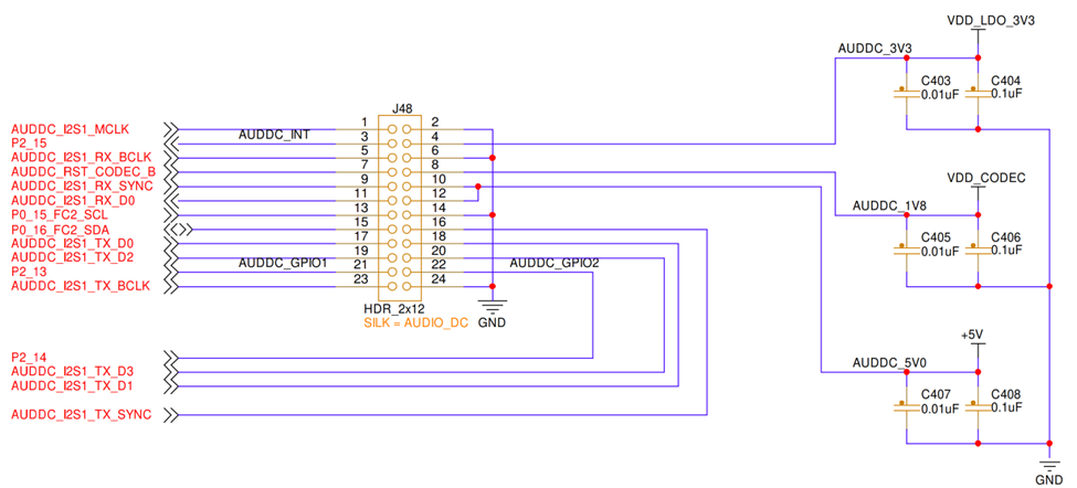
The audio expansion port is a simple 2x12 header with 2mm spacing. It provides access to a pair of FLEXCOMM ports, one for transmit and one for receive. The FLEXCOMM module in NXP devices is a flexible serial port which can be configured for many common serial interfaces. This includes all the common digital audio formats used with audio ADCs and DACs.
An audio master clock (MCLK) is available on the daughter card interface as well as some GPIO which supports interrupts and an I2C bus. Voltage rails of +5V, +3.3V and +1.8V are available for powering circuitry.
I used the +1.8V rail for setting the IO levels of the CS5366 and the +3.3V rail for powering the digital section of the data converter.
Figure 11. Audio Daughtercard Interface on the RT685-AUD-EVK
There are a handful of considerations when connecting external data converters to the RT685-AUD-EVK. The CS5366 supports TDM (Time Division Multiplexing) mode.
We will discuss this in a bit more detail later but the TDM is similar to the I2S in that it requires a data signal, a bit clock, a word select / frame sync and an audio master clock. All the TDM signals can be available on the daughter card expansion header but are routed by default to the onboard codec. There are solder jumpers on the RT685-AUD-EVK that can be used to route specific signals to expansion port.
Another important consideration when connecting to the daughter card interface is the IO levels on the signals. The i.MX RT685 provides a great deal of flexibility in how its IO banks are configured. The RT685-AUD-EVK defaults to 1.8V IO levels for the codec signals.
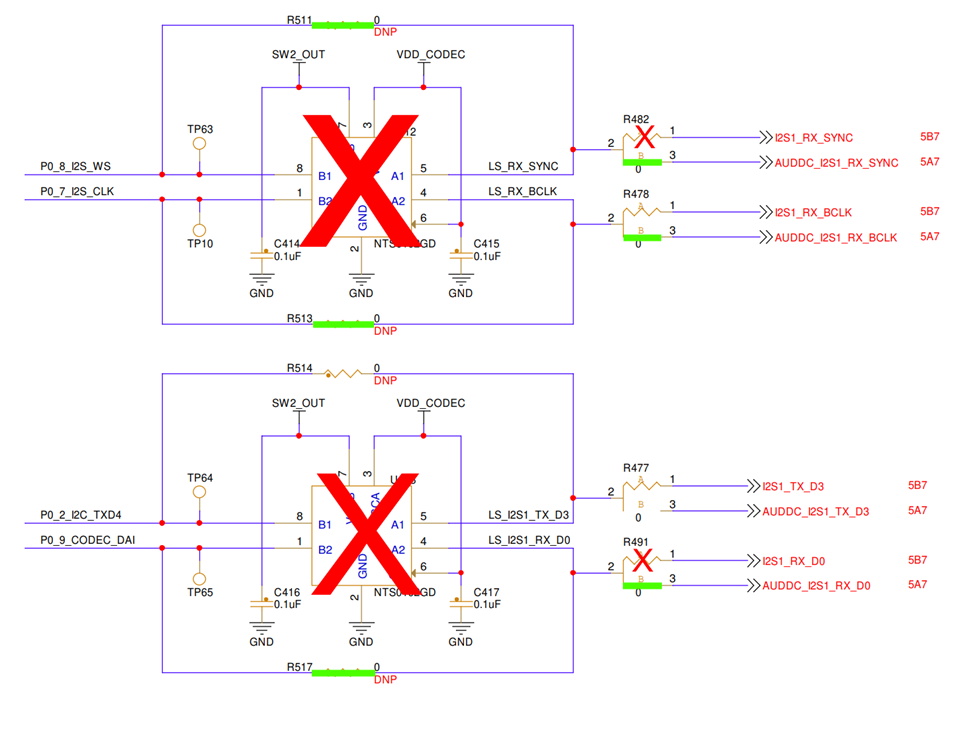
There are NTS0102GD bi-directional level shifters on the RT685-AUD-EVK to support level translation. However, I found that this part did not support +3.3V level translation in certain configurations. The CS5366 supports +1.8V IO levels through a dedicated IO power pin. I chose to bypass the level translators on the RT685-AUD-EVK and directly connect the RT685 IO to the CS5366 with +1.8V levels
Figure 12. Level Translator Bypass and Signal Routing to the Daughter Card Interface (Snippet from the RT685-AUD-EVK Schematic).
Page 6 of the RT685-AUD-EVK schematic shows all the routing options of the audio signals to the audio expansion port.
Since I only needed the FLEXCOMM Rx for the CS5366, I just configured the resistors for the signals I needed. I chose to bridge the MCLK jumper, so it gets routed to the external codec through expansion port and to the onboard CS42488 codec.
Figure 13. MCLK Routing (Snippet from the RT685-AUD-EVK Schematic).
I used the onboard codec for its DAC section only. Routing MCLK to the onboard and offboard data converters will allow me to use both devices simultaneously.
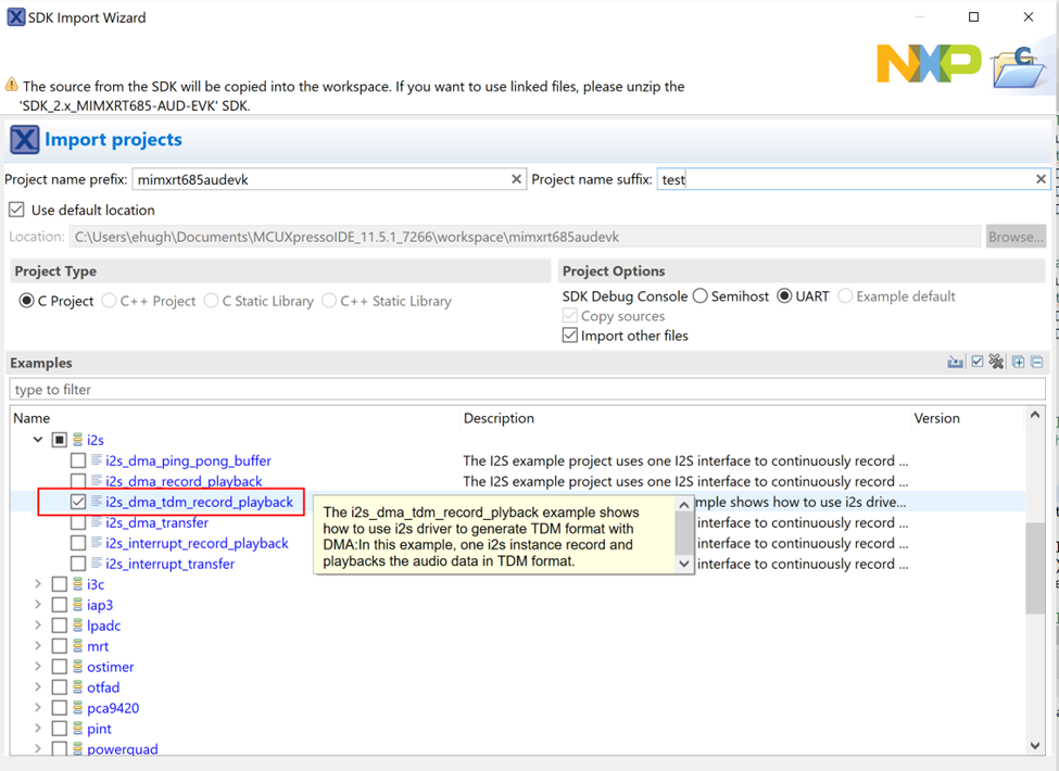
The MCUXpresso SDK has sample projects to support the RT685-AUD-EVK. There is a project that we can use to get data flowing from the external daughter card with minimal changes i2s_dma_tdm_record_playback. This i2s_dma_tdm_record_playback example initializes the onboard CS42488 codec to loop the ADC inputs to the DAC outputs. Using this a starting point, I can make some modifications to the FLEXCOMM receive channel to support the CS5366 and still loop data to the onboard DAC.
Figure 14. i2s_dma_tdm_record_playback sample in the RT685 SDK.
The onboard CS42488 is a combination six-channel ADC and DAC. It uses time division multiplexing (TDM) formatting for transmitting/receiving data. TDM can be thought of as an extension to the I2S (Inter-IC Sound) protocol. If you are not familiar with I2S, I would recommend starting w/ the NXP I2S documentation:
This document is essentially the original Phillips Semiconductor (which later became NXP Semiconductors) specification and illustrates how it works via shift registers. TDM samples are aligned to a frame sync (FS) signal. In some documentation this is also referred to as left/right clock (LRCLK) or word select (WS).
In the case of I2S, there is an underlying assumption of a two-channel pair. One sample gets transmitted when the Word Select (WS) / Frame Sync (FS) is high and the other sample is transmitted when the Frame Sync is low. For TDM audio, the bit clock is increased so that multiple samples are stuffed in the stream over the Frame Sync period.
This style of audio interface is simple to implement in hardware as the transmitter and receivers use shift registers at their core. The CS42488 and the CS5366 use similar formats for TDM.
There is one small difference that must be accounted for when initializing the FLEXCOMM interface for each of these devices. The CS42488 Frame Sync (documented as LRCK) is one bit clock wide pulse at the start of a group of audio samples:
Figure 15. CS42488 TDM Format.
The CS5366 requires a 50% duty cycle Frame Sync signal where half of the samples fit under the high period and the other half during the low period. The CS5366 outputs data for 8 samples per frame, however only the first six are valid.
Figure 16. CS5366 TDM Format.
To modify the i2s_dma_tdm_record_playback to support the CS5366, there are two small modifications required. The first is to modify the width of the word select signal. The default setting in the i2s_dma_tdm_record_playback example is set to l2S_ModeDspWsShort which is a single pulse at the beginning of a frame. Simply change to kI2S_ModeDspWs50.
Figure 17. CS5366 TDM Format Modification in the i2s_dma_tdm_record_playback MCUXpresso SDK sample.
On my daughter card, I intended to operate the CS5366 in 256x oversample mode over a TDM slave interface. This means that the master clock needs to be 256x the desired sample rate. The example software configured the sample rate to be 48kHz, which is the same rate the WS signal toggles. This translates into a 12.288MHz master clock requirement.
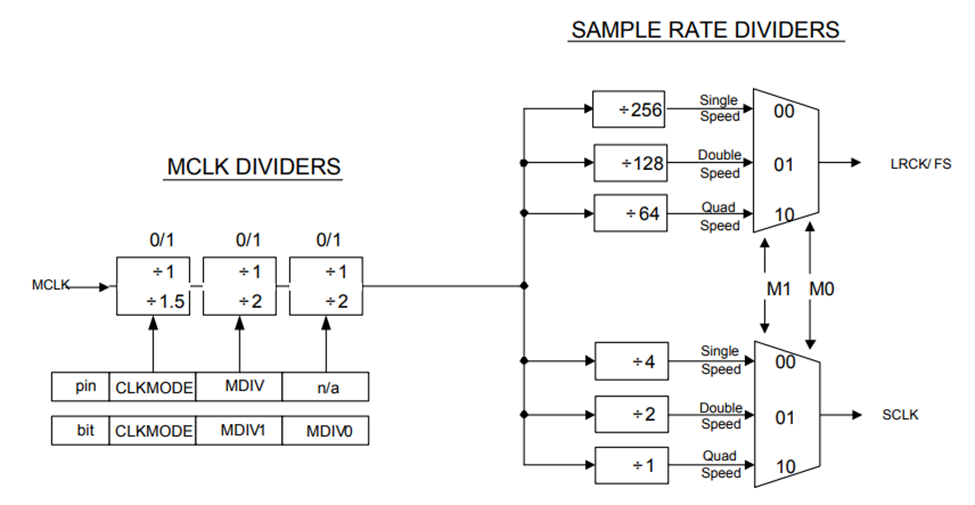
Sample rates for professional audio codecs such as the CS5366 are typically set by the ratio between the incoming master clock and Word Select/Frame Sync signals. Once these are set, one can determine what the bit clock is needed to be to shift out all the samples in one Frame Sync period. For example, if our desired sample rate is 48kHz and there are eight 32-bit samples for each frame, the bit clock needs to be (48000 x 8 x 32) Hz.
In this case, the bit clock is 12.288MHz which is the same as our leader clock. Every codec has rules about what MLCK to WS/FS to BCLK/SCK ratios are allowed. Check your codec data sheet to understand which MCLK ratios are supported.
Figure 18. CS5366 MCLK Configuration and Allowed Clock Ratios in TDM Slave.
Since I am using the CS5366 in TDM slave mode, the RT685 just needs to feed in a correct master clock, bit clock and Frame Sync signals, and the data will appear on the data out pin.
The i2s_dma_tdm_record_playback sample configures the audio PLL in the RT685 for 25.576MHz using the MCUXpresso Clocks tool, we can adjust the audio PLL to our target of 12.288MHz. The MCUXpresso Clocks tool is powerful in that you can specify the target frequency and the dividers/parameters can be auto adjusted.
Figure 19. Audio Master Clock Adjustment using MCUXpresso Clocks Tool
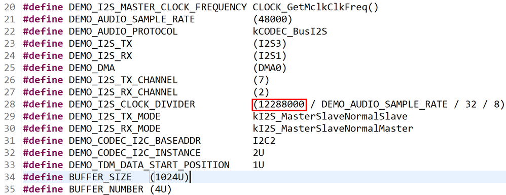
We also need to patch a value in the i2s_dma_tdm_record_playback sample to ensure the clock divider in the FLEXCOMM is correct. The sample code had the master clock frequency hardcoded in a macro and we need to change it to ensure correct operation.
Figure 20. Patching the i2s_dma_tdm_record_playback sample for 12.288MHz Master Clock.
With these changes, we can program the EVK and see data flowing from the CS5366.
Using a Saleae logic analyzer, I captured the bit clock, Frame Sync (shown as WS) and data output.
Figure 21. CS5366 Data Output on the Daughtercard.
From the logic analyzer capture, you can see the WS signal toggling and data for six channels being output in the first six slots.
Completing the Audio Engineering Test Bed
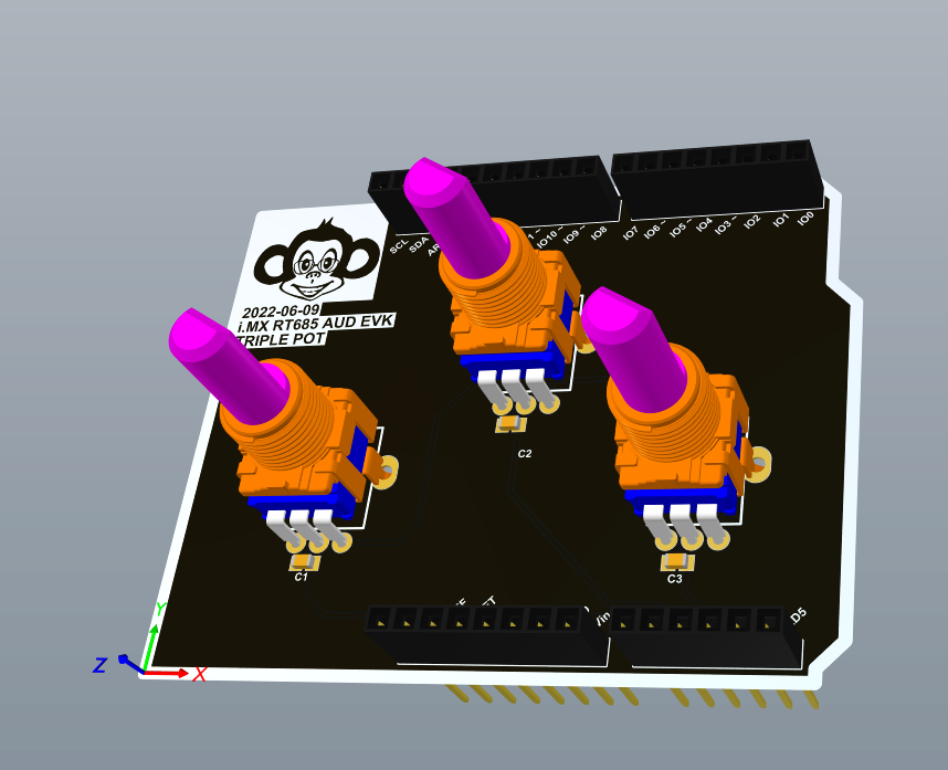
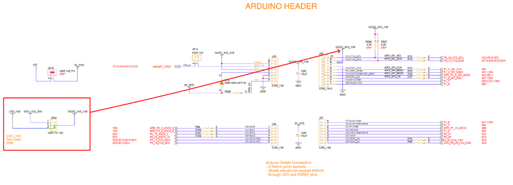
The RT685-AUD-EVK has Arduino style headers for adding additional “shields” to further access I/O on the RT685. To complete my test bed with the RT685-AUD-EVK, I elected to use the ADC built into the RT685 to sample three potentiometers for audio controls. I built a simple PCB with 3 potentiometers in an Arduino shield form factor.
Figure 22. Triple Potentiometer Arduino Shield for the RT685-AUD-EVK.
An important point to consider when using the Arduino headers are the IO levels. In my previous i.MX RT685 articles (see links at the end of this article), I stepped through a basic hardware design using the RT685. The analog subsystem is fundamentally based upon 1.8V IP. The IOREF pin on the shield interface is selectable via jumpers on the RT685-AUD-EVK. Ensure that your circuit will not apply more than 1.8V to the analog input channels.
Figure 23. AREF Level selection on the RT685-AUD-EVKArduino Shield Interface.
I also found that two of the analog I/O pins I was using on the Arduino headers were routed through a digital level translator. I removed this translator and populated the proper zero-ohm jumper to route the signal to the I/O pin of the RT685.
Figure 24. Digital Level Translator Bypass for Analog IO pins on the Arduino Shield Interface.
The translator on the RT685-AUD-EVK was populated to support digital functions on the Arduino header. Be sure to check the signal path of any I/O you may use to ensure correct levels.
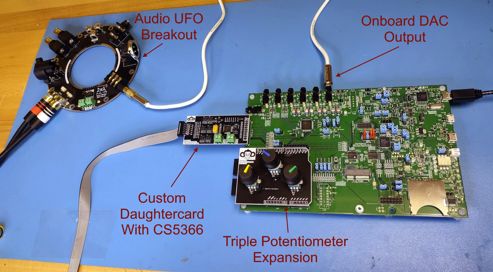
Putting all the pieces together, I have a test bed for developing audio processing algorithms.
Figure 25. Digital Audio Engineering Test Bed using the RT685-AUD-EVK, a Custom Daughter Card, and an Arduino Shield for Audio Controls.
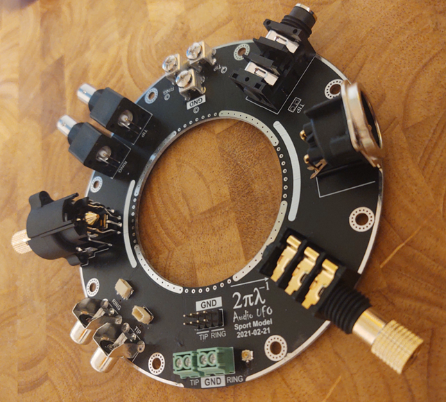
I even got to use my “Audio UFO” breakout board. The Audio UFO was a breakout board I designed to be able to adapt to all the most common jack styles. I even included some “not so common” connectors to be able to tap into analog audio signals. This allows flexibility in connecting test equipment when monitoring my processed analog outputs.
Figure 26. Audio UFO Breakout Board.
The RT685-AUD-EVK allowed me to validate my custom front end circuitry and get started on other critical DSP software development. I was able to connect the piezoelectric saddle pickups on my engineering guitar into the test bed via the custom daughtercard. From here I can focus on firmware in the MCU and DSP cores in the RT685.
If you are new to the i.MX RT685, I prepared several articles that highlight all the interesting features in this crossover MCU and what makes it a great audio development platform. I also illustrated how to bring up a minimal configuration hardware design to help get your own system up and running faster. This includes a core schematic, PCB layout and even how to bring up the Zephyr real-time operating system. All the i.MX RT685 articles are linked at the end of this article.
Visit the i.MX RT685-AUD-EVK home page here to learn more and get started.
Cheers!
Links to additional i.MX RT685 Content:
Crossing Over With the i.MX RT600 Part 1 of 2
Crossing Over With the i.MX RT600 Part 2 of 2
i.MX RT685 Hardware Design 1 of 3 - Power and Package
i.MX RT685 Hardware Design 2 of 3 - Flash Memory and Boot Configuration
i.MX RT685 Hardware Design 3 of 3 - The SuperMonkey Design
i.MX RT685 SuperMonkey QSPI Bringup with MCUXpresso and Segger J-Link
Creating a Custom Zephyr Board for the i.MX RT685 SuperMonkey
You must be a registered user to add a comment. If you've already registered, sign in. Otherwise, register and sign in.
-
101
6 -
communication standards
4 -
General Purpose Microcontrollers
23 -
i.MX RT Processors
46 -
i.MX Processors
51 -
Interface
1 -
introduction
14 -
LPC Microcontrollers
73 -
MCUXpresso
34 -
MCUXpresso Secure Provisioning Tool
1 -
MCUXpresso Conig Tools
30 -
MCUXpresso IDE
42 -
MCUXpresso SDK
26 -
Model-Based Design Toolbox
6 -
MQX Software Solutions
2 -
QorIQ Processing Platforms
1 -
QorIQ Devices
5 -
S32N Processors
4 -
S32Z|E Processors
6 -
SW | Downloads
8 -
日本語ブログ
6
- « Previous
- Next »

