- NXP Forums
- Product Forums
- General Purpose MicrocontrollersGeneral Purpose Microcontrollers
- i.MX Forumsi.MX Forums
- QorIQ Processing PlatformsQorIQ Processing Platforms
- Identification and SecurityIdentification and Security
- Power ManagementPower Management
- MCX Microcontrollers
- S32G
- S32K
- S32V
- MPC5xxx
- Other NXP Products
- Wireless Connectivity
- S12 / MagniV Microcontrollers
- Powertrain and Electrification Analog Drivers
- Sensors
- Vybrid Processors
- Digital Signal Controllers
- 8-bit Microcontrollers
- ColdFire/68K Microcontrollers and Processors
- PowerQUICC Processors
- OSBDM and TBDML
-
- Solution Forums
- Software Forums
- MCUXpresso Software and ToolsMCUXpresso Software and Tools
- CodeWarriorCodeWarrior
- MQX Software SolutionsMQX Software Solutions
- Model-Based Design Toolbox (MBDT)Model-Based Design Toolbox (MBDT)
- FreeMASTER
- eIQ Machine Learning Software
- Embedded Software and Tools Clinic
- S32 SDK
- S32 Design Studio
- Vigiles
- GUI Guider
- Zephyr Project
- Voice Technology
- Application Software Packs
- Secure Provisioning SDK (SPSDK)
- Processor Expert Software
-
- Topics
- Mobile Robotics - Drones and RoversMobile Robotics - Drones and Rovers
- NXP Training ContentNXP Training Content
- University ProgramsUniversity Programs
- Rapid IoT
- NXP Designs
- SafeAssure-Community
- OSS Security & Maintenance
- Using Our Community
-
- Cloud Lab Forums
-
- Home
- :
- Model-Based Design Toolbox (MBDT)
- :
- NXP Model-Based Design Tools Knowledge Base
- :
- Interacting with Digital Inputs/Outputs on MR-CANHUBK344
Interacting with Digital Inputs/Outputs on MR-CANHUBK344
- Subscribe to RSS Feed
- Mark as New
- Mark as Read
- Bookmark
- Subscribe
- Printer Friendly Page
- Report Inappropriate Content
Interacting with Digital Inputs/Outputs on MR-CANHUBK344
Interacting with Digital Inputs/Outputs on MR-CANHUBK344
1. Introduction
In this series of articles, we demonstrate how to program the MR-CANHUBK344 board using the Model-Based Design Toolbox.
The goal of this first article is to briefly present the hardware setup (the board and the connections that have to be made) and offer step-by-step instructions on how to create, configure and upload a simple program on the MR-CANHUBK344 development board.
This article’s application consists of toggling onboard LEDs using the push button by configuring the Dio peripheral and the respective pins.
The next articles in the series will showcase how to use different peripherals of the MR-CANHUBK344 board.
1.1. The MR-CANHUBK344 board
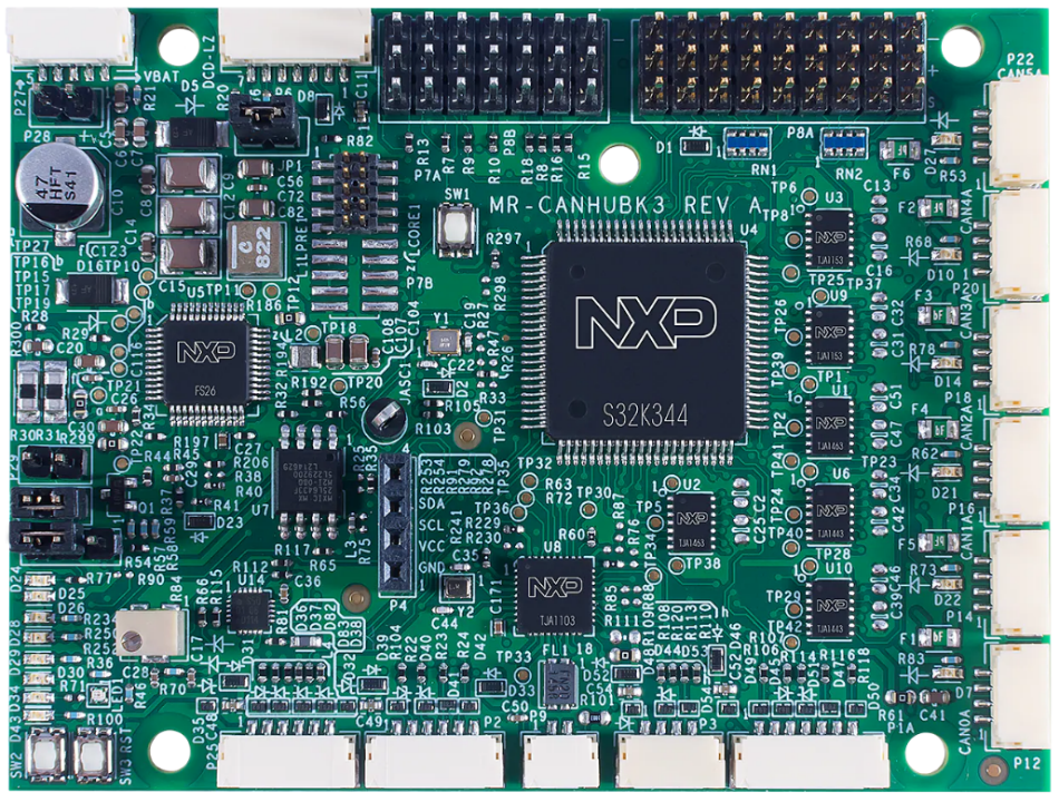
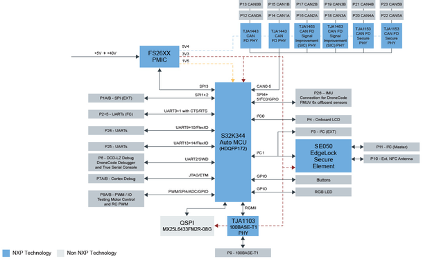
The MR-CANHUBK344 evaluation board provides a T1 ethernet interface alongside 6 CAN (Controller Area Network) interfaces, two for each of the three different types, CAN-FD (Flexible Data-Rate), CAN-SIC (Signal Improvement Capability) and CAN-SCT (Secure CAN Transceiver). The board is designed for mobile applications, and it is based on the NXP® S32K344, an Arm® Cortex®-M7 general-purpose automotive microcontroller, which features advanced safety, security and software support.
Below you can find the block diagram for the MR-CANHUBK344 board.
For more details about the MR-CANHUBK344 board, please follow the link:
https://www.nxp.com/design/development-boards/automotive-development-platforms/s32k-mcu-platforms/s3...
1.2. Prerequisite Software
To be able to follow the steps in this article, the following software is necessary:
- MATLAB® and Simulink® (2021a or newer), including Stateflow®, MATLAB® CoderTM, Simulink® CoderTM, Embedded Coder®
- Model-Based Design Toolbox for S32K3xx 1.4.0
1.3. Prerequisite Hardware
During this example, the following hardware is used:
- MR-CANHUBK344 evaluation board
- J-Link Debug Probe
- 12V power supply and adapters to allow powering up the board through the P27 port
1.4. Powering up the MR-CANHUBK344
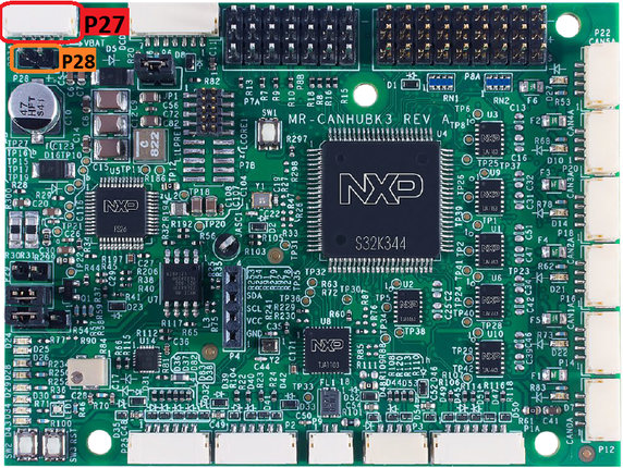
First, the CANHUBK344 board accepts a wide range of input voltages, from 5V to 40V, which can be delivered through 2 different ports.
- P27 is the main power delivery port and it is used with a 5-pin JST-GH connector. This connector has 2 lines for power, 1 is not connected and the last 2 are ground lines.
- P28 is an alternate way of powering up the board and it consists of a 2-pin header.
Regardless of the port chosen for powering up the board, precautions should be taken to make sure that the polarity is correct and that the pins align properly with the ports.
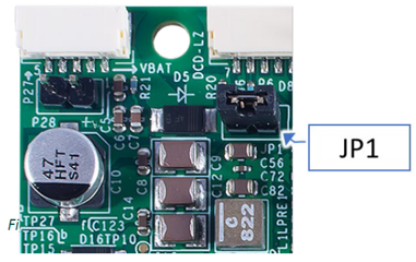
Note: By default, the FS26 PMIC (Power Management IC) implements a challenger window watchdog that will reset the board’s MCU continuously if the challenge is not handled in software. To avoid this behavior, the FS26 must be put into debug mode. This is done by removing the JP1 jumper, then supplying 12V to the board and then inserting the JP1 jumper again.
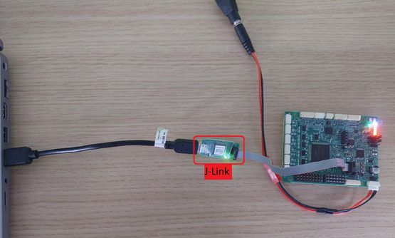
An example of how to connect both the power supply and the J-Link Debug probe will be discussed in the next chapter.
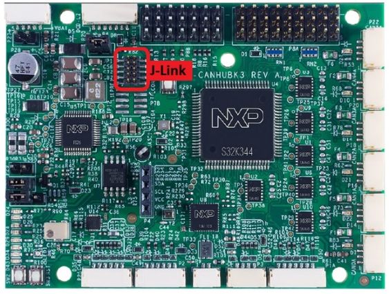
1.5. Connecting the J-Link Debug Probe
When connecting the J-Link Debug Probe, pay attention to the connector, to make sure that you are aligning the red stripe of the connector with the pin number 1 on both sides.
The associated J-Link software is not included in the Model-Based Design Toolbox and has to be installed separately. Installing the J-Link's software in the default location will allow it to work without having to select the location of the installation every time a new model is created.
2. Digital Inputs/Outputs Configuration
So far, we have covered details about the board, how to power it up and how to connect the J-Link Debug Probe to it. This chapter will focus on designing the application that will run on the MR-CANHUBK344 board using the Model-Based Design Toolbox.
2.1. Creating and configuring the Simulink model
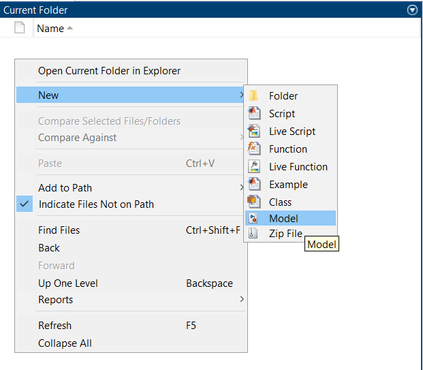
Create a new model:
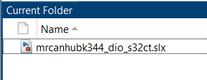
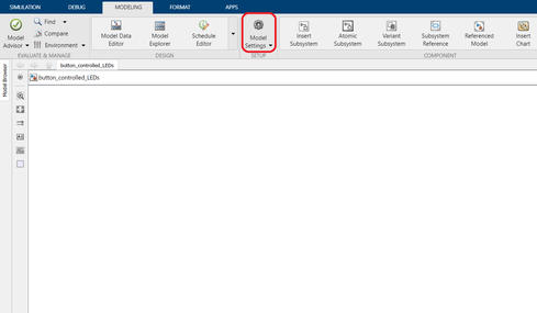
Next, open the newly created model and head to the MODELING tab. To configure the hardware, click on the Model Settings option. If you have a tough time finding the button, you can use the Ctrl+E shortcut to open the Model Settings window.
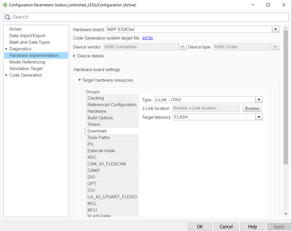
Moving forward, the correct Hardware board must be chosen from the Hardware Implementation tab. In this case, it is NXP S32K3xx.
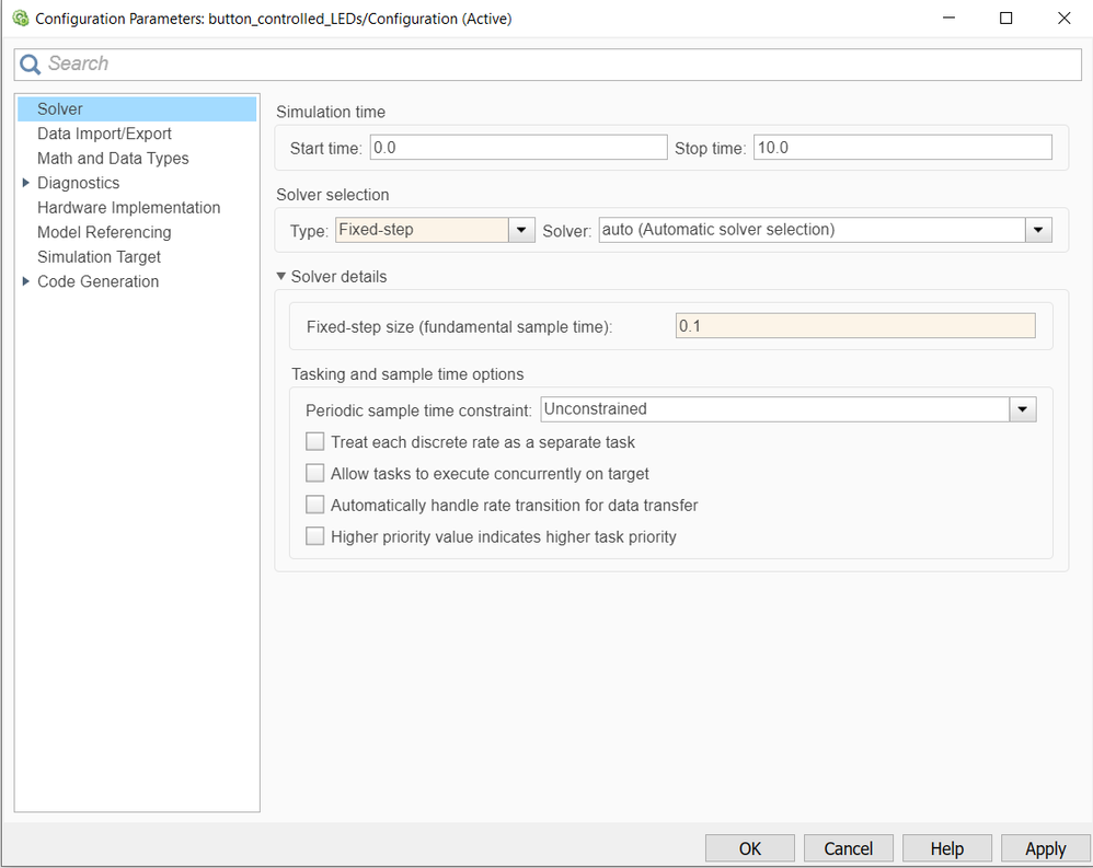
On the Solver tab, make sure to configure the Type to Fixed-step and set the Fixed-step size according to the needs of the application. This parameter controls how often the code in the model runs by setting the period time.
For example, a Step Size of 0.1s would make the code run 10 times in a second, once every 0.1 seconds. In the current project, this value ends up affecting the frequency of the LED that is being toggled by itself, so setting it to a very small value might make it hard to see that the LED is indeed blinking. Setting it to a higher value would make the buttons feel unresponsive because the code would check for button presses rarely. A good value for this example is 0.1s, because the toggling LED will be ON, and respectively OFF 5 times in a second, since it changes every 0.1 seconds. This way, the LED’s change is visible, and the buttons feel responsive because their interaction is checked every 0.1 seconds.
A few more options must be configured in Hardware Implementation. First, to access the submenu needed for the next changes, you have to click on the Target hardware resources option. From there, select Hardware and change the Hardware Part to S32K344-Q172. This will load the default configuration for the S32K344-Q172 hardware part. Later we will modify this configuration to work on the MR-CANHUBK344.
Afterwards, head to the Download tab, still under the Target hardware resources submenu. Make sure that the Type is set to J-Link – JTAG and that the Target Memory is set to FLASH. If your J-Link software has been installed in a location that is different from the default location, you have to select the path to the JLink.exe executable by pressing the Browse button next to the J-Link location label and selecting the executable from the location where it was installed.
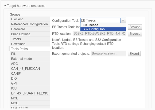
The last step in the Target hardware resources submenu is to navigate to the Tools Paths and select S32 Config Tool in the Configuration Tool field. This setting changes the external configuration tool that will be used to configure the MCU’s pins, clocks and peripherals. This will allow the MCU to properly control all the components of the board. The Model-Based Design Toolbox for S32K3 uses integration with dedicated configuration tools to allow the configuration of the board's pins, clocks and peripherals, providing options for both Elektrobit Tresos (EB Tresos) and S32 Configuration Tools. More details on this configuration will be provided in the following sections.
After all the changes have been made, do not forget to click Apply and Ok.
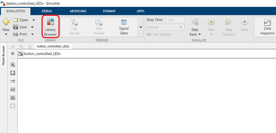
Now, we are going to start designing the application model. To access the Model Based Design Toolbox provided blocks that control the hardware, click on the Library Browser button, which is going to open the Simulink Library Browser.
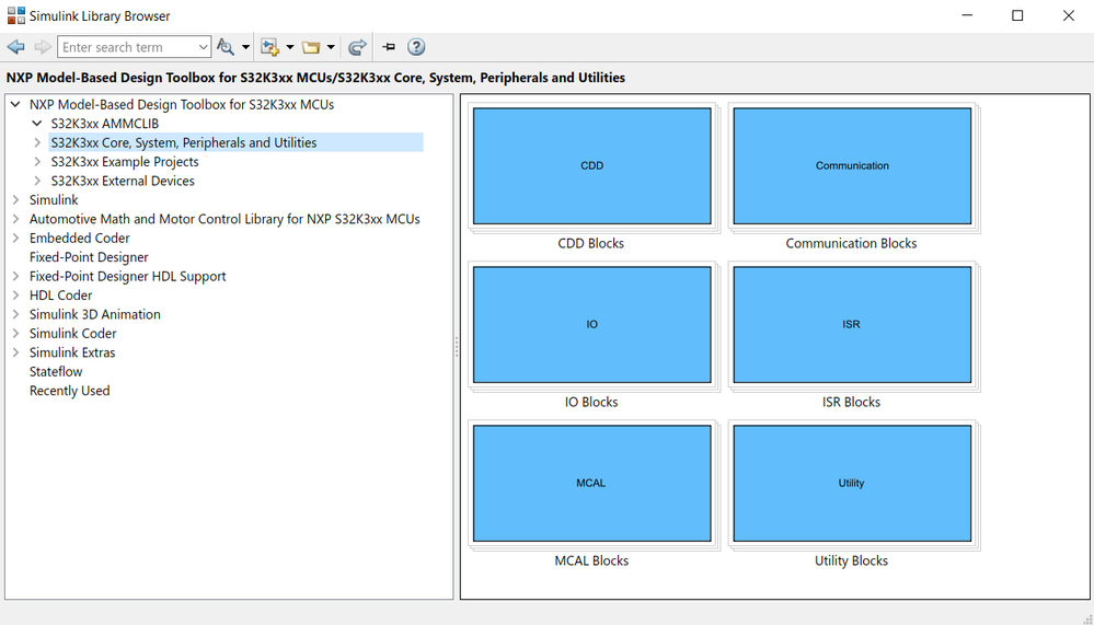
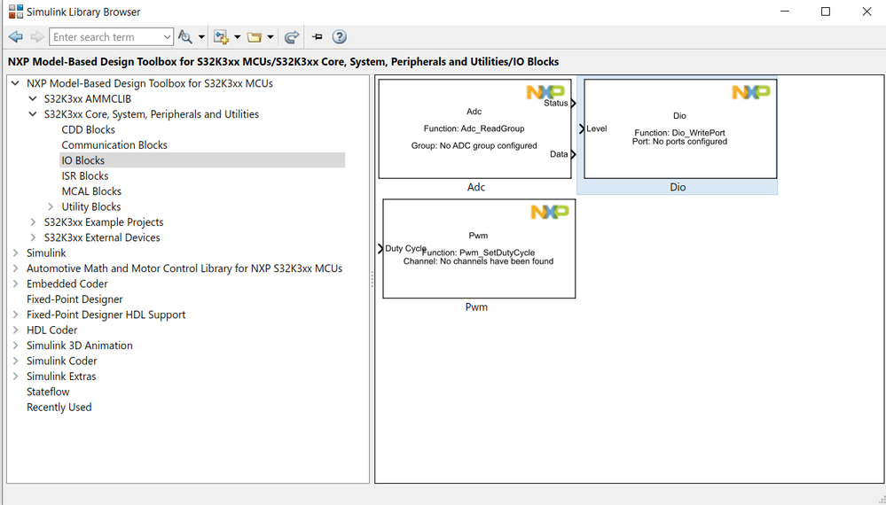
From this window, navigate to the S32K3xx Core, System, Peripherals and Utilities menu under the NXP Model-Based Design Toolbox for S32K3xx MCUs and then select the IO Blocks from the right side of the window.
In this example we will only use Dio blocks, so to start things off, we can drag-and-drop the Dio block into the Simulink Workspace.
For the blocks to control the right pins, we must use the external configuration tool chosen to map the pins to the correct values.
When creating an application for a supported Hardware Part, the Model-Based Design Toolbox comes with a default configuration project, enabling an initial set of peripherals, pins and clock settings for all the components it offers support for. The toolbox can be used with this default configuration project to design applications, without requiring any additional steps inside external configuration tools.
However, if the hardware or the application requires a different configuration than the default one, the external configuration tools allow you to open and modify the default configuration project to suit your needs.
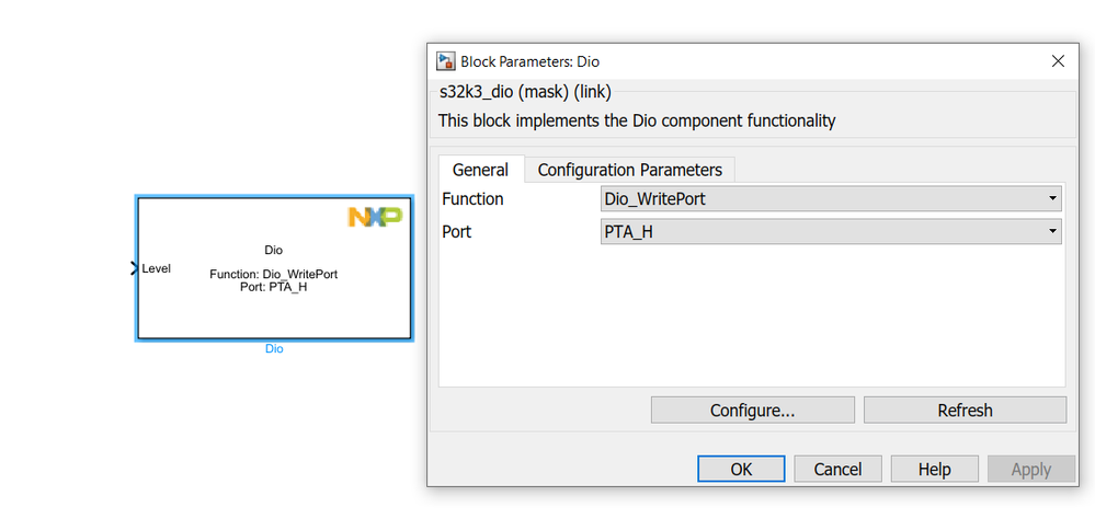
To quickly open the S32 Config Tool, you can double-click on the Dio block that has just been added and then click on the Configure… option. This opens the project’s configuration in the selected configuration tool.
The configuration can also be done in EB Tresos in a similar manner, if it is the designated configuration software.
2.2. Pins Configuration
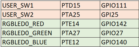
The next step is to take note of the pins used for the project you intend on creating. In this example, we will be using 2 LEDs and one of the 2 push buttons available on the board, which are part of the Dio component. By studying the schematic, we can obtain all the information we need about the pins used.
To be able to easily find a pin, search for its name and then look for the correspondence. In this example, by looking for the USER_SW1 pin, we can see that it is assigned to the PTD15 pin, also identified as GPIO111.
After doing this for every pin, we can proceed with the configuration.
While using the S32CT program, the pins’ MSCR (third column) will not be needed, but they will be required for the EB Tresos configuration.
First, we will have to configure the pins to work as we expect them to, as inputs, outputs or even both. To do that, navigate to the Pins Tool by clicking on the Pins button.
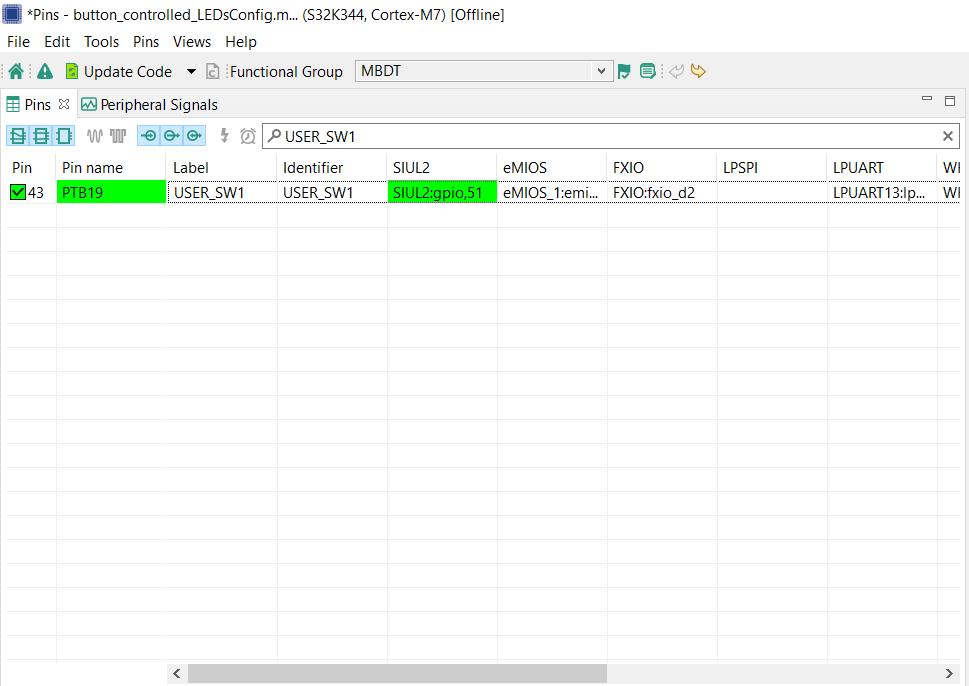
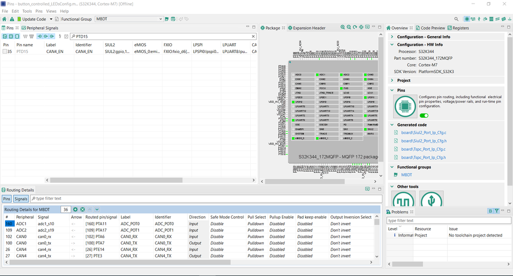
In this step, we will focus our attention on the top-left window, the Pins tab. First, we must check if there is any pin with the same name in the configuration. To do that for the button named USER_SW1 we can type its name value in the type filter text field.
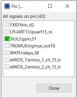
Here we can see that a pin with the same name already exists, and it is configured on the pin PTB19. To avoid further configuration issues, we must disable this pin. We can do that by clicking on the green Checkbox from the left side of the row. Then, we deselect the already selected item and click done, making sure nothing else is selected.
To start the configuration process for the first pin, the button named USER_SW1, we can type its pin value in the type filter text field.
As we can see, the pin is not configured for our intended behavior. To change that, we must update the identifier, the label, and click on the checkbox on the left. By doing that, the following menu will pop up:
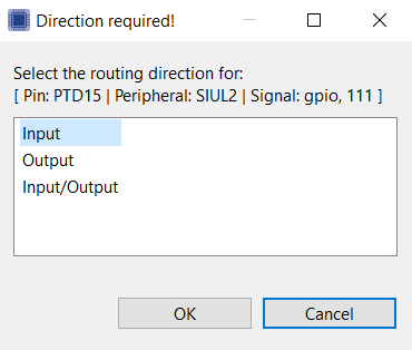
Here we will select the SIUL2:gpio,111 option since it matches our requirement. Afterwards, another window will pop up asking about the direction of the pin. In this case, we are configuring a button, so we only expect it to act as an Input.
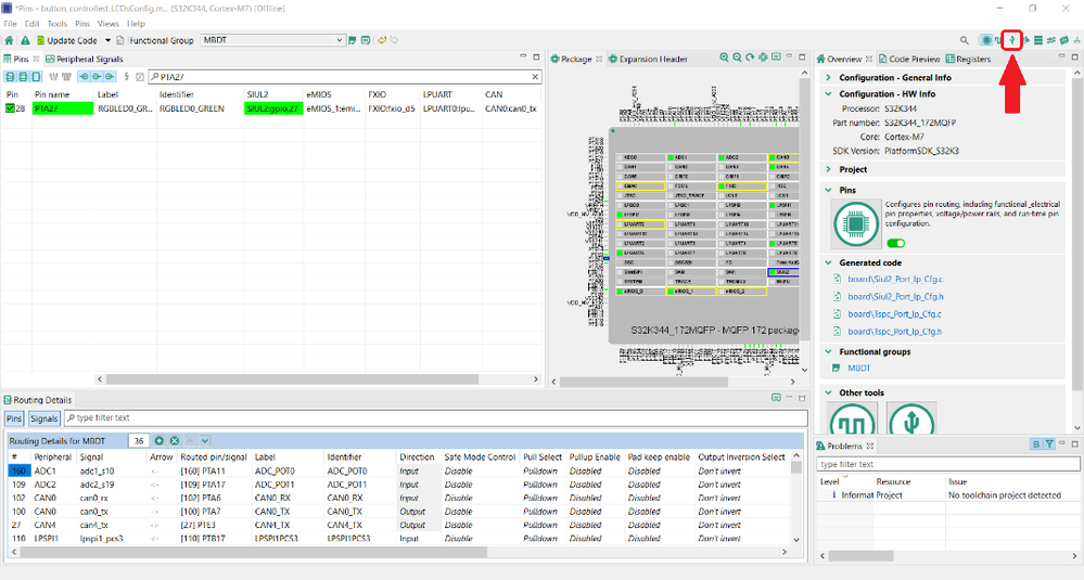
This process of removing the old configuration and adding the new one has to be repeated for every pin that will need to be configured. Keep in mind that when configuring the LEDs, you will have to set the direction as Input/Output since one of the LEDs will be toggled from one state to another, which requires the LED to be read before the output can be inverted.
By taking a look at the bottom window, Routing Details, we can see more configuration options for the pins. You can use the type filter text field to limit the results to only the pins you are interested in seeing. The MR-CANHUBK344 board has its LED logic inverted, so, by default, the board's LEDs would turn on when powering the board. To avoid that, we assign an Initial Value to the LED. By setting the Blue LED's Initial Value to High, it is going to turn off as soon as the board starts.
2.3. Component Configuration
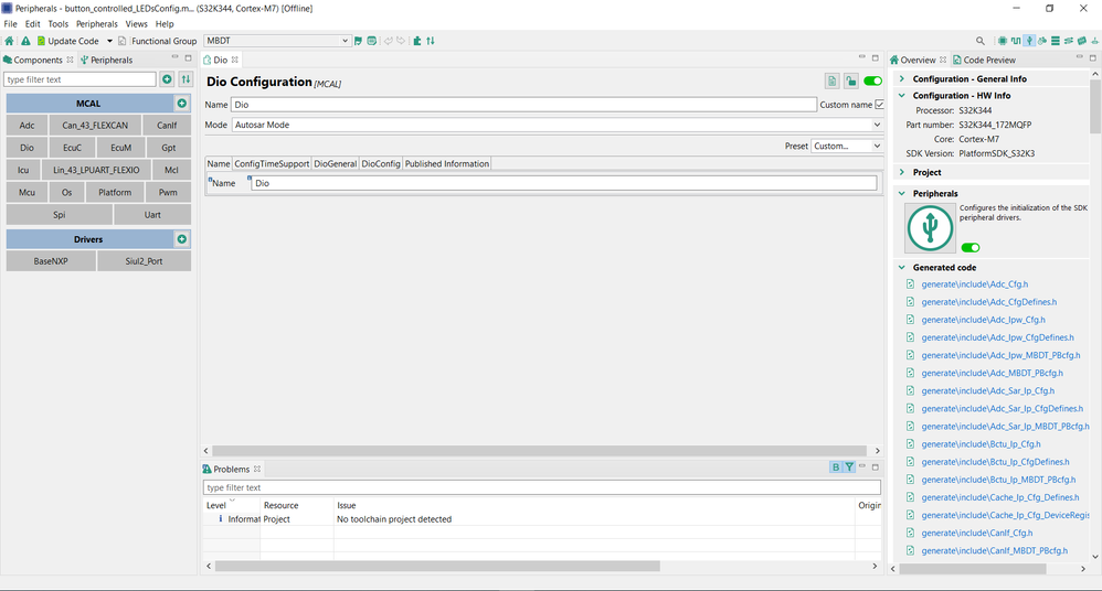
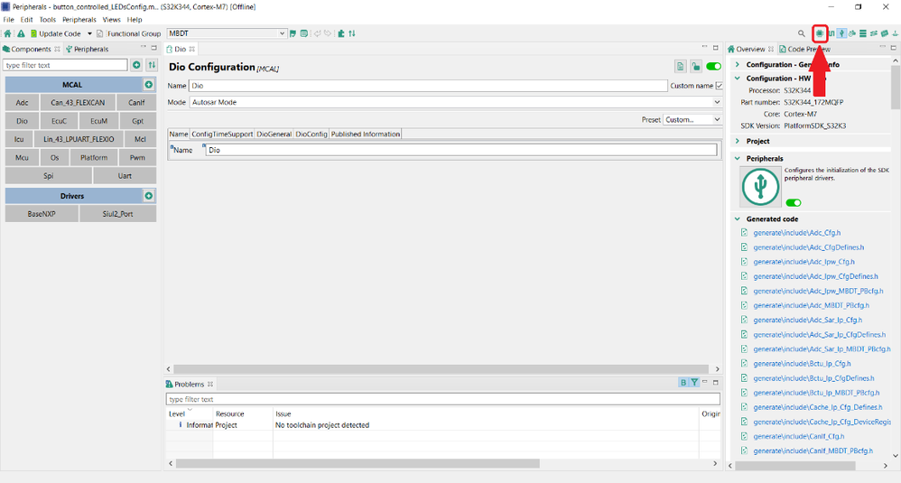
Head back to the Peripherals Tool by clicking on the Peripherals button.
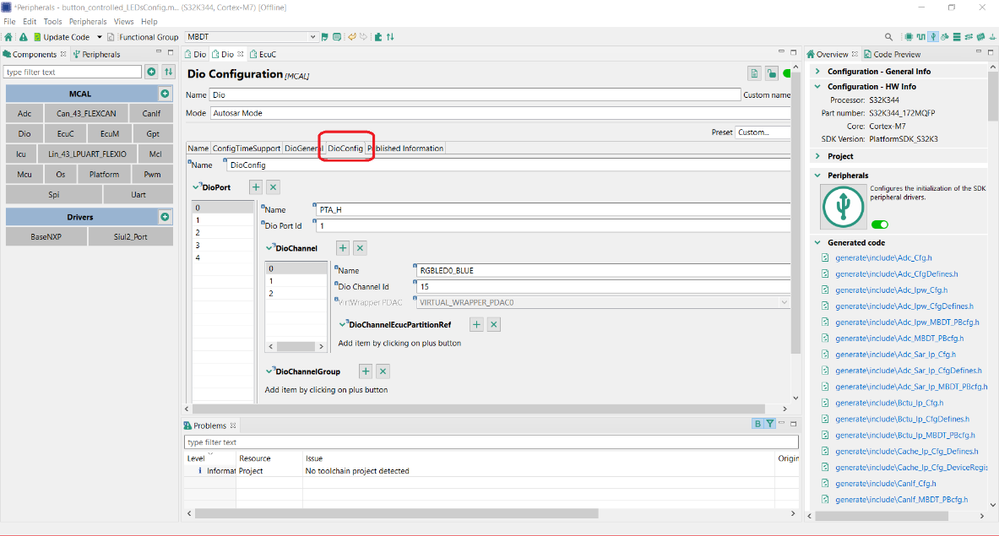
Finally, after configuring the pins’ directions, we have to configure the Dio component so that the pins can be used during the execution of the program. This will be done in the DioConfig tab under the Dio Configuration tab. If it is not showing by default, you can press on the Dio component on the left side of the screen and it should bring it up.
Understanding how the DioPort and DioChannel are organized might prove useful later. The number present under the DioPort label represents the corresponding value of the Dio port that you want to access. Below you can find a table with the correspondence between the values and the registers.
|
AL=0 |
AH=1 |
|
BL=2 |
BH=3 |
|
CL=4 |
CH=5 |
|
DL=6 |
DH=7 |
|
EL=8 |
EH=9 |
Each of those is half of a register and together every line forms a 32-bit register. For example, AL and AH contain all the pin values that are assigned to PTA. AL contains the first 16 pins and AH contains the next 16 pins.
For example, the RGBLED0_GREEN pin is assigned to PTA27. From that we can conclude that, since 27 is higher than 15 (the 16th value of AL, since the first value is 0), the PTA27 pin must be assigned to the AH register.
To reiterate, the PTA0-PTA15 pins belong to the AL register while the PTA16-PTA31 (the value must be offset by -16 when computing the Id) pins belong to the AH register, and this is true for the rest of the registers too, PTB, PTC, PTD, PTE.
Given that the previous configuration did not match our setup, we should first prepare the registers by removing the components that we have already disabled in the section 2.2.
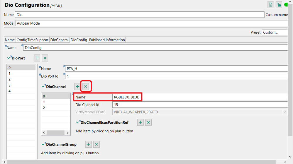
For example, in the DioPort 0 we can see the old (disabled) LEDs, which can be removed by clicking the X button shown. This should be done for each DioPort Id to make sure there aren’t any incorrectly configured items. In the current case, we only have to remove the RGBLED0_BLUE, RGLED0_GREEN and USER_SW_1 items, which we will later replace with our own.
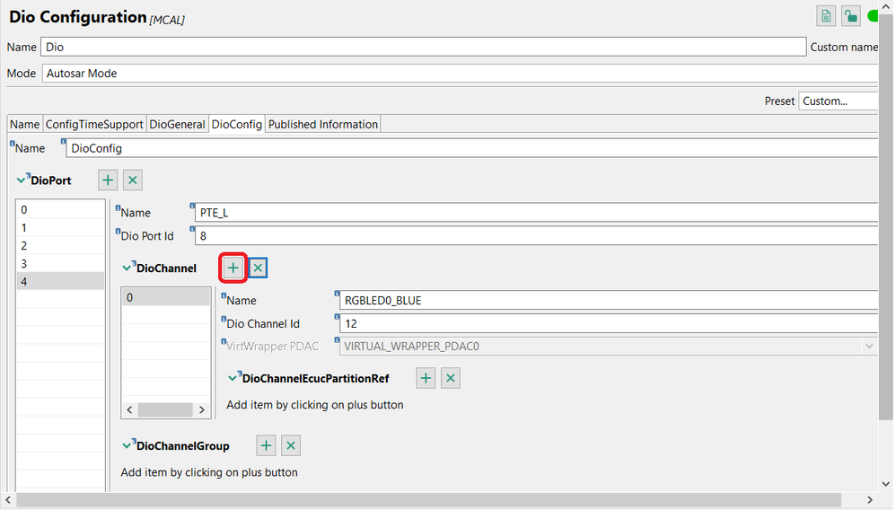
After removing the LEDs’ configuration from the previous ports, since now the LEDs are routed to different pins, we can start adding the pins that we have configured in the prior step. Figuring out where each pin should go relies on the explanations from the beginning of this chapter. As an example, adding the ping RGBLED0_BLUE, which corresponds to PTE12, means going to the DioPort 4 because the value 12 is found in the first interval, 0-15, which points us to the EL register.
To add a DioChannel, click on the + Button next to DioChannel. A new channel will be created and you have to fill in the details regarding the port.
This has to be done for every of the 3 configured pins, in their respective registers.
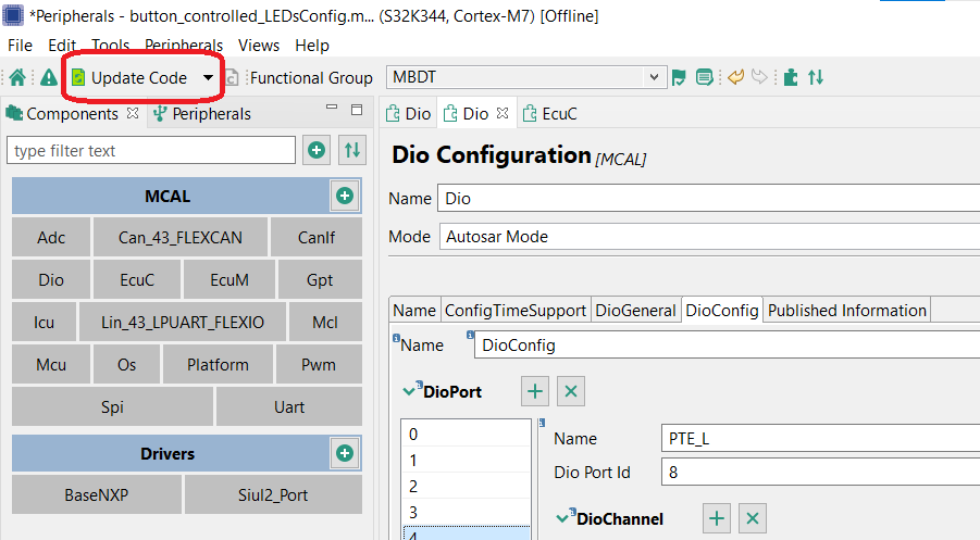
The last step is to save the configuration project and press the Update Code button. Afterwards, press Ok on the dialog window that popped up. Afterwards, feel free to close the configuration software.
To update the configuration in the Simulink model, press the Refresh button inside the menu that pops up when double-clicking a block.
3. DIO Model Overview
This article’s goal is to explain the workflow of creating a model that toggles the LEDs based on the push buttons available on the board. The logic will be the following:
- The blue LED is toggled using the Push button 1;
- The green LED is automatically toggled every simulation step.
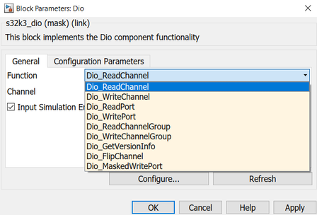
This means we will need blocks to read an input value, write an output value and flip an output value. These operations can be achieved using Dio blocks. A Dio block has multiple possible functions, which you can select from the Function dropdown. Once a new function is selected, the functionality and the block’s inputs and outputs will change accordingly.
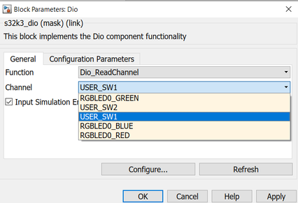
The pin that is going to be the target of the function can be chosen by selecting it from the dropdown list of the Channel option. The items that appear in the dropdown list correspond to the Dio channels that have been configured in chapter 2.3.
The Input Simulation Enable option will not be used in this example, so it should be unchecked. Enabling this option will create an additional input for the block, which can be used to simulate the model’s behavior. For the functions Dio_ReadChannel, Dio_ReadChannelGroup and Dio_ReadPort, the block outputs the simulation input. For the Dio_FlipChannel function, the block will output the inverted simulation input
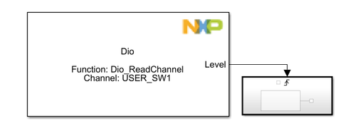
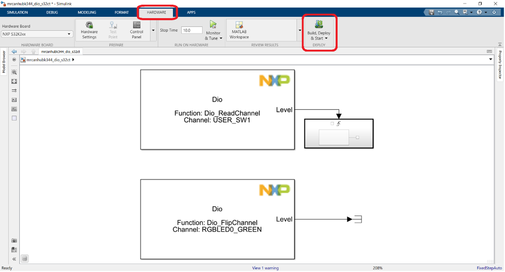
The way the Dio Block is currently configured, it will read the input value from the button USER_SW1 which we can later use to control the LEDs.
Since we want to toggle an LED when a button is pressed, it means we have to look for the rising edge of that input. To do that, a Trigger subsystem block will be used, that takes as input the value read from the button USER_SW1. The block’s Trigger type is configured to rising by clicking on the Trigger icon and when it detects that rising edge in its input, the subsystem will be executed. In this situation, we use the Dio block to invert the output of the LED.
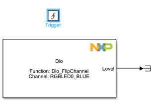
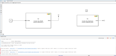
The contents of the newly added Trigger subsystem are seen below:
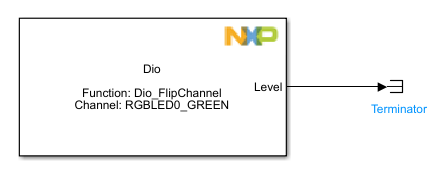
Automatically toggling the green LED is a much simpler task due to the function FlipChannel available in the Dio block. The FlipChannel Dio block also has an output, which outputs the current state of the LED. Since that information is not going to be used anywhere else, a Simulink Terminator can be attached to that output, to avoid having errors.
To upload and run the code on the MR-CANHUBK344 board, select the HARDWARE tab at the top of the window, and then click on the Build, Deploy & Start button. This will start the process of generating code from the Simulink model and uploading it to the board using the J-Link programmer.
Note: If the J-Link’s path was not configured in the earlier steps, a dialog box will pop up requiring the path to the executable. If the software was installed in the default location, pressing on the Default option will be enough.
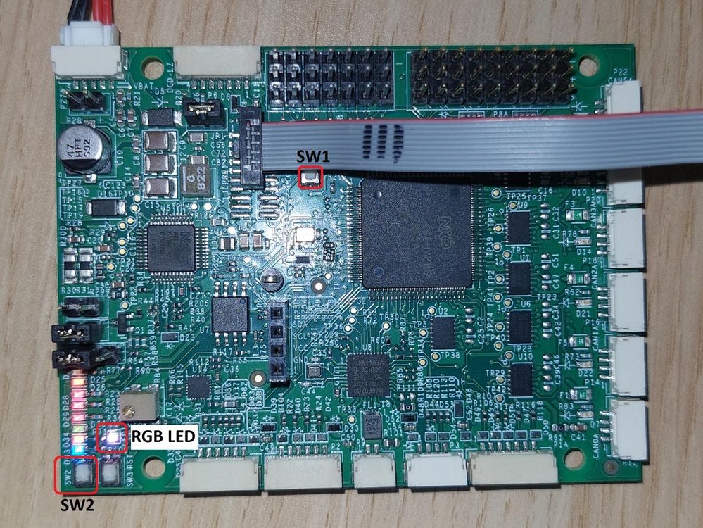
Initially, after uploading the program or resetting the board, you will notice that the RGB LED is green and blinking. Keep in mind that the MR-CANHUBK344 board has its LED logic inverted, so writing a value of 1 to an LED output will turn it off, and writing a value of 0 to an LED output will turn it on. Pressing the SW1 toggles the blue LED, while the green one keeps blinking.
4. Conclusion
After following the steps shown in this tutorial, you should now be able to create applications that use the MR-CANHUBK344 board’s LEDs and push buttons along with the Model-Based Design Toolbox.
To continue learning about the MR-CANHUBK344 development board and how it can be used with the Model-Based Design Toolbox, check out the next articles in this series:
- Beginner's Guide for Model-Based Design Toolbox: Sending data via UART and monitoring signals with F...
- Beginner's Guide for Model-Based Design Toolbox: Controlling LED intensity with ADC and PWM
- Beginner's Guide for Model-Based Design Toolbox: Communicating over the CAN Bus
Instructions on how to run the attached model:
- Download and extract the archive’s contents;
- Copy both the .mdl and .mex file to the location where you wish to set up the project;
Note: for the model to work properly, please place the .mex file next to the model. - Open the .mdl file and make sure that MATLAB’s Current Folder points to the folder that contains the model;
- Click on the Hardware tab and then press the “Build, Deploy & Start” button.
NXP is a trademark of NXP B.V. All other product or service names are the property of their respective owners. © 2023 NXP B.V. Arm, Cortex are trademarks and/or registered trademarks of Arm Limited (or its subsidiaries or affiliates) in the US and/or elsewhere. The related technology may be protected by any or all of patents, copyrights, designs and trade secrets. All rights reserved. MATLAB, Simulink, Stateflow and Embedded Coder are registered trademarks and MATLAB Coder, Simulink Coder are trademarks of The MathWorks, Inc. See mathworks.com/trademarks for a list of additional trademarks.
- Mark as Read
- Mark as New
- Bookmark
- Permalink
- Report Inappropriate Content
This article was super helpful for a beginner like me to work with the MR CANHUB S32K board.
Where can I find these two articles ? Or are they yet to be published?
- Beginner's Guide for Model-Based Design Toolbox: Sending data via UART and monitoring signals with F...
- Beginner's Guide for Model-Based Design Toolbox: Controlling LED intensity with ADC and PWM
Again, thank you for this really good example. This should be a really good example for beginners to start with.
- Mark as Read
- Mark as New
- Bookmark
- Permalink
- Report Inappropriate Content
Hello @HariRam_111 ,
The articles mentioned at the end will be uploaded in the coming weeks.
The second article should be published this friday, while the third one will be posted the next friday.
Regards,
Robert V
- Mark as Read
- Mark as New
- Bookmark
- Permalink
- Report Inappropriate Content
The second article in this series is now published:
Sending data via UART and monitoring signals with FreeMASTER
- Mark as Read
- Mark as New
- Bookmark
- Permalink
- Report Inappropriate Content
Hi, can you please add 2 more articles for MR-CANHUBK344 boards
1) SPI communication
2) CAN communication
- Mark as Read
- Mark as New
- Bookmark
- Permalink
- Report Inappropriate Content
Hello @ankitv ,
There is an article about CAN communication on the MR-CANHUBK344 board planned for the following weeks.
Regards,
Robert V
- Mark as Read
- Mark as New
- Bookmark
- Permalink
- Report Inappropriate Content
Thanks for the awesome article. @Adrian_Gherca @robertv
For the next subchapter of it, I want to use an external switch and an external LED. I want to connect the external switch on Pin 5 of the P8B header and the LED to Pin 8 of the P8B header.
Where can I find the corresponding PIN names for these 2 pins?
Where did you get the below detail from? it's missing in the SW and HW docs.
Thanks
- Mark as Read
- Mark as New
- Bookmark
- Permalink
- Report Inappropriate Content
Hello @ankitv ,
We are using the board's schematic to find out the pin names.
You can find it at https://www.nxp.com/design/development-boards/automotive-development-platforms/s32k-mcu-platforms/s3... if you go to the Design Resources section. Another resource that could come in handy is the PCBLayout included in the board's DesignPackage, which makes figuring out the P8B and P8A pins easier.
Let me know if this was useful or if you were looking for something else.
Regards,
Robert V
- Mark as Read
- Mark as New
- Bookmark
- Permalink
- Report Inappropriate Content
Hello Robert, Yes the above resource was useful. I was able to connect an external switch and an external LED using GPIO on P8B. Thanks
Regards,
Ankit
- Mark as Read
- Mark as New
- Bookmark
- Permalink
- Report Inappropriate Content
Hello Robert,
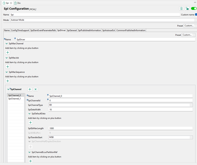
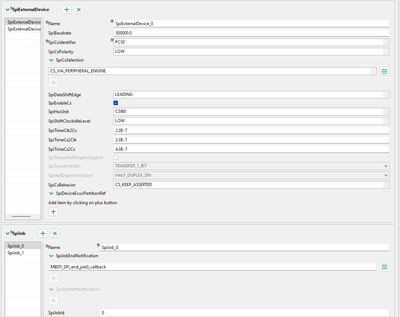
I want to send SPI data in the above example on button press. I have added Spi_WriteIB block and set the channel to 0.
I am trying to use the P1A port channel 0 for the signal. data is MSB first. Can you advise
1) How to change the configuration to 16bits?
2) How do I do peripheral config for SPI to use P1A port channel 0
Regards,
Ankit
- Mark as Read
- Mark as New
- Bookmark
- Permalink
- Report Inappropriate Content
Hi,
I have a question about your project. If I only want to achieve the file .bin but I don´t know how achieving it. I know that I have to use "embedded coder" or "simulink coder". Could you tell me the steps to achieve it, please?
Thanks you for all,
Jon Ander Amante Jorge
- Mark as Read
- Mark as New
- Bookmark
- Permalink
- Report Inappropriate Content
Thanks for the great examples @robertv !
Is there a comprehensive manual for the S32K configurator? I'm finding that it's a very powerful tool but without detailed documentation, it's tricky to navigate.
- Mark as Read
- Mark as New
- Bookmark
- Permalink
- Report Inappropriate Content
Hello @LyingCake ,
I am glad to hear that you found these articles useful.
Regarding your question about additional resources, apart from these 4 articles around the MR-CANHUBK344 board, we have a few other articles on specific components, like the ones found in the right side of the MBDT Community page: https://community.nxp.com/t5/Model-Based-Design-Toolbox-MBDT/bd-p/mbdt.
To clarify things a bit, you are referring to the S32 Configuration Tool, when used with the Model-Based Design Toolbox, right? If you are looking for something more specific, let me know and I'll try to find some resources.
Regards,
Robert V
- Mark as Read
- Mark as New
- Bookmark
- Permalink
- Report Inappropriate Content
Thanks for directing me to the community page @robertv
My specific question is- if there are multiple channels within a group, how would you read each individual channels? The output of the Adc_ReadGroup block is a single uint16, regardless of how many channels are configured within the group. Would I need to create a new group for each channel?
