- Forums
- Product Forums
- General Purpose MicrocontrollersGeneral Purpose Microcontrollers
- i.MX Forumsi.MX Forums
- QorIQ Processing PlatformsQorIQ Processing Platforms
- Identification and SecurityIdentification and Security
- Power ManagementPower Management
- Wireless ConnectivityWireless Connectivity
- RFID / NFCRFID / NFC
- MCX Microcontrollers
- S32G
- S32K
- S32V
- MPC5xxx
- Other NXP Products
- S12 / MagniV Microcontrollers
- Powertrain and Electrification Analog Drivers
- Sensors
- Vybrid Processors
- Digital Signal Controllers
- 8-bit Microcontrollers
- ColdFire/68K Microcontrollers and Processors
- PowerQUICC Processors
- OSBDM and TBDML
- S32M
-
- Solution Forums
- Software Forums
- MCUXpresso Software and ToolsMCUXpresso Software and Tools
- CodeWarriorCodeWarrior
- MQX Software SolutionsMQX Software Solutions
- Model-Based Design Toolbox (MBDT)Model-Based Design Toolbox (MBDT)
- FreeMASTER
- eIQ Machine Learning Software
- Embedded Software and Tools Clinic
- S32 SDK
- S32 Design Studio
- GUI Guider
- Zephyr Project
- Voice Technology
- Application Software Packs
- Secure Provisioning SDK (SPSDK)
- Processor Expert Software
-
- Topics
- Mobile Robotics - Drones and RoversMobile Robotics - Drones and Rovers
- NXP Training ContentNXP Training Content
- University ProgramsUniversity Programs
- Rapid IoT
- NXP Designs
- SafeAssure-Community
- OSS Security & Maintenance
- Using Our Community
-
- Cloud Lab Forums
-
- Knowledge Bases
- ARM Microcontrollers
- i.MX Processors
- Identification and Security
- Model-Based Design Toolbox (MBDT)
- QorIQ Processing Platforms
- S32 Automotive Processing Platform
- Wireless Connectivity
- CodeWarrior
- MCUXpresso Suite of Software and Tools
- MQX Software Solutions
- RFID / NFC
-
Guide to designing antennas for the NTAG I2C plus
Guide to designing antennas for the NTAG I2C plus
This post entry provides a guide to designing antennas for the NTAG I2C plus. This article has been structured as follows:
- How the NTAG I2C plus works
- NTAG I2C plus antenna design files
- Basic antenna theory for NTAG I2C plus tags
- NTAG I2C plus electrical input capacitance
- Antenna coil electrical equivalent circuit
- Tag with an NTAG I2C plus electrical equivalent circuit
- Antenna design procedure for NTAG I2C plus tags
- Design the antenna coil
- Measure the antenna coil parameters
- Calculate the resonant capacitor value
- Assemble and measure resonant frequency
- Example: Tuning for a 54x27mm PCB antenna
- Summary
- Further information
- Video recorded session
How the NTAG I2C plus works
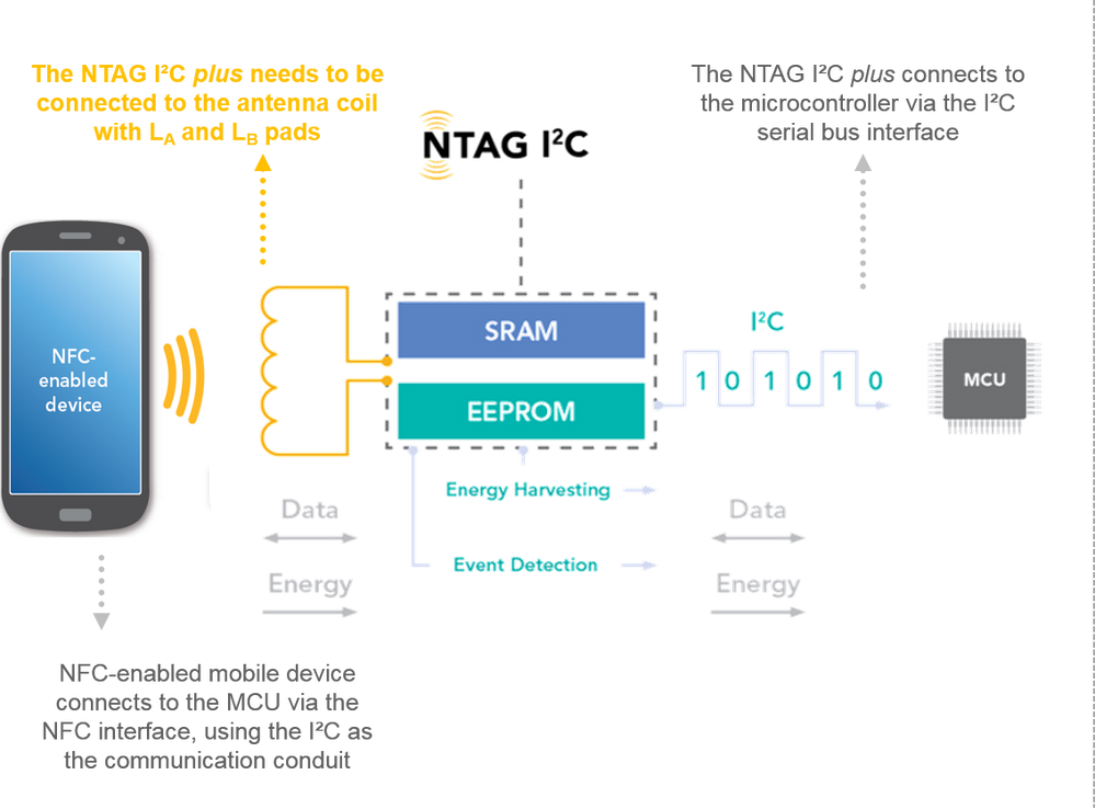
The NTAG I2C plus is what we call a connected NFC tag. It combines a memory, a passive NFC interface and a contact I2C interface. Additionally, it has more features such as:
- A field detection pin, to send a wake-up signal to a connected MCU
- The Energy harvesting, able to power external devices
- The SRAM, a memory without writing cycles limitation
- The pass-through mode, for fast data exchange between interfaces
- Memory access control options, available from both NFC and I2C interfaces
- And the originality signature, to protect your brand against clones
As such, it supports bidirectional communication between an NFC-enabled device and the host MCU and it is an ideal solution for Industrial applications, IoT nodes, meters, consumer electronics and accessories among others.
To enable the NFC interface, the chip needs to be connected to an antenna coil using the two dedicated antenna pins. How to design this coil is the main goal for today.
NTAG I2C plus antenna design files
The NTAG I2C plus support package includes development kits, demo apps, sample code, application notes, and, the design files of the Class 4 PCB antenna, and the Class 6 Flex antenna, which are available for direct and free download from the website. 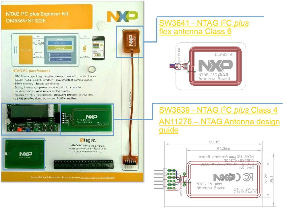
include:
- The schematics
- The Gerbers
- The BoM
Therefore, if you do not have any antenna size or shape constrains in your application, the easiest is to just copy & paste these reference antennas.
On the other hand, if you need to design your custom antenna, NXP also offers a coil design Excel sheet to help you. I will talk more about it along the article.
Basic antenna theory for NTAG I2C plus tags
The NTAG I2C plus is an 8-pin package, with:
- The field detection pin
- The Vout pin
- The I2C serial clock and data Iines to the MCU
- The ground
- The VCC
wo antenna pins
NTAG I2C plus electrical input capacitance
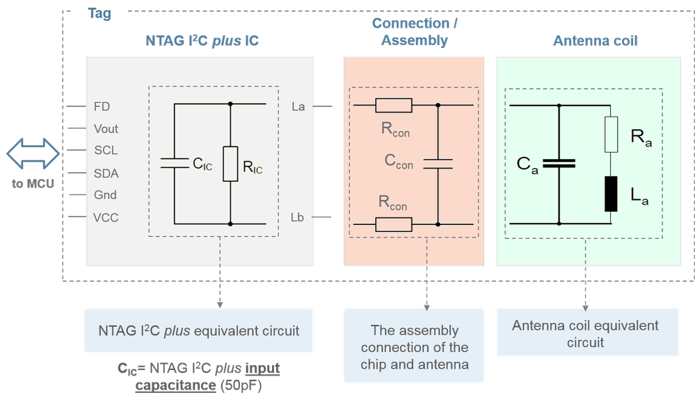
The NTAG I2C plus equivalent circuit can be represented with:
- A resistor, representing its current consumption
- And a parallel capacitor, representing the chip internal capacitance
For the NTAG I2C plus, this capacitance is 50pF for both the 1k and 2k memory versions. Precisely, the chip capacitance is the most important factor for the antenna tuning.
Antenna coil electrical equivalent circuit
The antenna coil itself is a resonant circuit with an input impedance. The electrical equivalent model of the antenna coil consists of:
- An inductance
- A capacitance
- And some resistive losses of the loop antenna itself.
The actual impedance value depends on:
- The antenna material
- The thickness of the turns, mainly affecting the resistance
- The distance between the windings, mainly affecting the capacitance
- The number of turns, mainly affecting the inductance
- And the nearby environment
Tag with an NTAG I2C plus electrical equivalent circuit
When the NTAG I2C chip and the antenna coil are assembled, we can consider a parasitic resistance and capacitance generated by the connections between the chip and the antenna. This parasitic impedance depends on the assembly process used and the antenna material.
As a result, what we can observe in the schematic of the figure is that the NTAG I2C plus capacitance together with the parasitic connection capacitance and the antenna capacitance forms a resonance circuit with the inductance of the antenna
coil.
The self-resonance frequency of a system is given when the imaginary part of the circuit equivalent impedance is null, and the system is only purely resistive.
Considering the antenna loop inductance, the parallel equivalent capacitance and the parallel equivalent resistance of the tag, the resonance frequency and the quality factor of the tag can be calculated by these formulas.
Antenna design procedure for NTAG I2C plus tags
The antenna design procedure for the NTAG I2C plus tags is:
- Design the antenna coil. This is about the antenna specs in terms of number of turns, track width, spacing, shape, etc according to your application requirements.
- Characterize the antenna coil and find its R, L, and C parameters.
- Calculate the parallel capacitor value required to adjust the tag resonant frequency
- Assemble the calculated capacitor and measure the results. If the results are not accurate enough, fine-tune the capacitor value, assemble and measure again as needed.
Design the antenna coil
As part of the ISO14443 standard, six PICC antenna classes are defined. Per each of the antenna class, the physical characteristics and dimensions are defined. For instance, Class 1 is the largest, with a size comparable to the size of a regular credit card, and Class 6, which is the smaller one. In addition, Class 3 to Class 6 define two antenna shapes: a rectangular and a circular one. However, tag manufacturers are not constrained to conform to any of these dimensions. Therefore, its use is optional and rather intended to improve interoperability. As such, you may consider using these antenna sizes as a reference for your designs.
The major parameter of the antenna coil is the inductance. This inductance can be estimated based on geometrical parameters and the material properties such as:
- The diameter for a round antenna or the overall length and width for a rectangular shape.
- The track width
- The gap between track
- The thickness
- And the number of turns
To avoid cumbersome formulas, NXP offers you an Excel-based coil calculation tool to estimate the inductance of rectangular and circular antennas. This tool uses some parameters related to the material used and the antenna dimensions. And with it, it estimates the antenna inductance for you. Typically, the coil design steps include:
- An estimation of the electrical parameters, like the operating frequency and the chip capacitance
- The definition of the target inductance, we define the dimensions, the track width, the gap between track, the thickness, etc that achieves our target inductance.
- The production of prototypes. Based on the matrix run, with different inductance values deviated between 10-20% plus and minus the original value.
- Characterization of the coil prototypes. Based on this characterization, select the one with the best parameters for your application. If needed, you can execute a second matrix run, with new prototypes, based on the first results.
Measure the antenna coil parameters
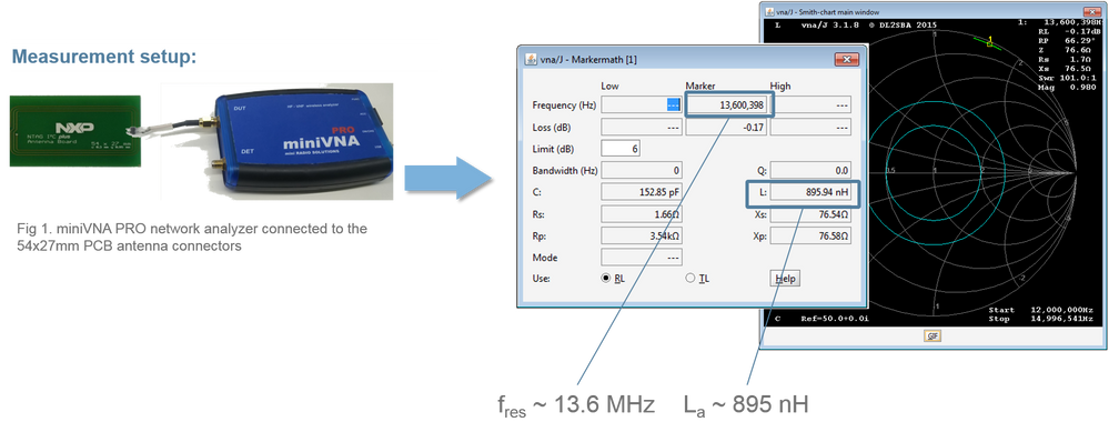
The antenna characterization can be done using a network analyzer connected to the antenna pads, isolated from the rest of the circuit. For our case, a low-end solution, such as the miniVNA PRO is sufficient. This device is cheap compared with the high-end devices like Agilent but still, accurate enough for our needs.

Calculate the resonant capacitor value
We use a network analyzer to measure the system resonant frequency after connecting the NTAG I2C plus to the antenna coil. As I explained before, the self-resonant frequency of the tag is given when the system is purely resistive. Most likely, the actual resonant frequency will not be 13.56MHz as we would like, but some other value. If that is your case, calculate the system capacitance at the current resonant frequency based on the equation derived from the NFC tag equivalent circuit shown previously.

- We know the current resonant frequency
- We know the antenna inductance, because we measured it before with the network analyzer
- And, as design parameter, we define the target resonant frequency
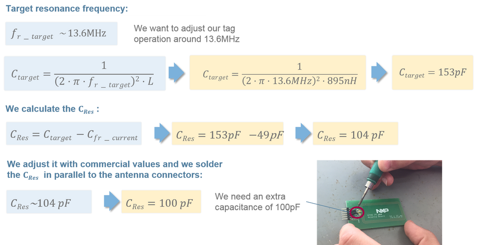
With this data, we can use once again, this formula to calculate which is the resulting capacitance that would make our tag resonate to our target resonant frequency. Knowing the required total capacitance and the actual capacitance, we can calculate the extra capacitance missing. This is given by this formula:
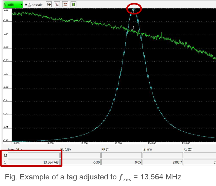
Regarding the target resonant frequency, for single tag operation, a tuning slightly above 13.56 MHz would lead to maximum read-/write distance. However, due to manufacturing tolerances, a nominal frequency up to 14.5 MHz would still operate well.
Assemble and measure resonant frequency
Therefore, the last steps are:
- Solder the capacitor in parallel
- Connect the network analyzer
- And measure the new resonant frequency
If the resonant frequency measured is not the target one, repeat the process by fine tuning the capacitor value. If the frequency is higher than expected, you can increase the capacitor value. On the other hand, if the frequency is lower than expected, you can decrease it.
Example: Tuning for a 54x27mm PCB antenna
Based on a real lab exercise, this section illustrates the steps to adjust the tuning of an antenna for the NTAG I2C plus.
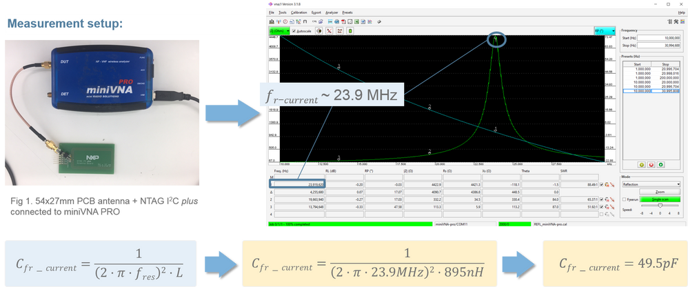
As described before, we need to start by characterizing our antenna coil. In this lab exercise, we have used a PCB antenna of 54 by 27 mm and, we have connected our miniVNA PRO to the antenna pads. The results that we have obtained from this measurement are that our PCB antenna has an inductance around 895 nH.
After characterizing the antenna coil:
- We have soldered the NTAG I2C plus chip to this PCB antenna.
- Right after, we connect again the miniVNA PRO to measure the actual resonant frequency.
In this case, it returns a resonant frequency near 24 MHz. Using the formula, we calculate that the tag capacitance at 24 MHz is almost 50 pF. Note that, the actual capacitance is basically the chip capacitance as the antenna and connection capacitance is usually not impacting significantly.
Obviously, a resonant frequency of 24MHz is way too high for a ISO14443 NFC tag like our NTAG I2C plus. Therefore, we need to add some capacitance to the system so that we can bring this resonant frequency down. As an example, for this lab exercise, we are adjusting the tag to around 13.6 MHz, intentionally a bit higher than the NFC operating frequency. With a target resonant frequency to 13.6MHz and an antenna inductance is around 895nH, the result is that the tag needs a total capacitance of around 153 pF. This means that we need to solder an extra capacitance of 100pF to bring down the resonant frequency. So we go to our component box, and select the closer commercial value (100pF).
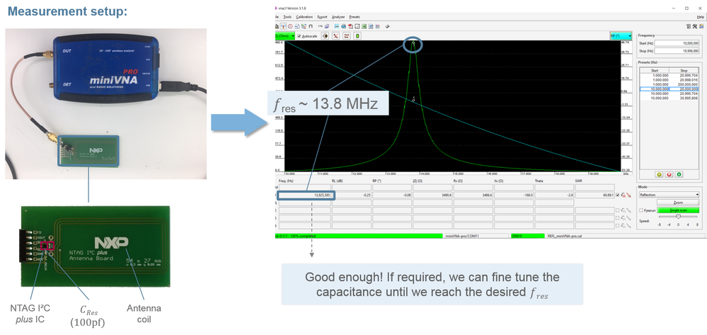
As a last step, it is worth to measure how well adjusted is our system after adding the 100pF. We connect the miniVNA to the system including the IC, the antenna and the 100pF. Now, the results obtained are that the resonant frequency is 13.8 MHz. In our case, we consider this as good enough. However, you are always free to repeat this process as many times as needed until you obtain the accuracy that you need.
Summary
The antenna tuning steps for the NTAG I2C plus that we followed are:
- Design the antenna coil. You can use the NXP reference antennas or design your own antenna coil using the NXP Excel-based calculation tool.
- Measure the antenna coil. Use a network analyzer connected to the antenna pads, without any other circuitry
- Calculate the extra capacitance. Measure the current resonant frequency, and we calculate the extra capacitance needed to achieve the desired operating frequency.
- Solder and measure. If the results are sufficient, you are done. Otherwise, repeat the process with a new capacitance value
As you can see, the antenna tuning process is quite straight forward. Basically, it is a matter of adjusting the capacitance of the tag until the operating frequency is the right one.
Further information
You can find more information about NFC in:
- NTAG I2C plus website http://www.nxp.com/products/:NT3H2111_2211
- NTAG antenna design guide support package https://www.nxp.com/docs/en/application-note/AN11276.zip
- NXP technical community: https://community.nxp.com/community/identification-security/nfc
- NXP design partners: https://nxp.surl.ms/NFC_AEC
Video recorded session
On 25 July 2018, a live session explaining this topic was delivered. You can watch the recording here:
