- NXP Forums
- Product Forums
- General Purpose MicrocontrollersGeneral Purpose Microcontrollers
- i.MX Forumsi.MX Forums
- QorIQ Processing PlatformsQorIQ Processing Platforms
- Identification and SecurityIdentification and Security
- Power ManagementPower Management
- MCX Microcontrollers
- S32G
- S32K
- S32V
- MPC5xxx
- Other NXP Products
- Wireless Connectivity
- S12 / MagniV Microcontrollers
- Powertrain and Electrification Analog Drivers
- Sensors
- Vybrid Processors
- Digital Signal Controllers
- 8-bit Microcontrollers
- ColdFire/68K Microcontrollers and Processors
- PowerQUICC Processors
- OSBDM and TBDML
-
- Solution Forums
- Software Forums
- MCUXpresso Software and ToolsMCUXpresso Software and Tools
- CodeWarriorCodeWarrior
- MQX Software SolutionsMQX Software Solutions
- Model-Based Design Toolbox (MBDT)Model-Based Design Toolbox (MBDT)
- FreeMASTER
- eIQ Machine Learning Software
- Embedded Software and Tools Clinic
- S32 SDK
- S32 Design Studio
- GUI Guider
- Zephyr Project
- Voice Technology
- Application Software Packs
- Secure Provisioning SDK (SPSDK)
- Processor Expert Software
-
- Topics
- Mobile Robotics - Drones and RoversMobile Robotics - Drones and Rovers
- NXP Training ContentNXP Training Content
- University ProgramsUniversity Programs
- Rapid IoT
- NXP Designs
- SafeAssure-Community
- OSS Security & Maintenance
- Using Our Community
-
- Cloud Lab Forums
-
- Home
- :
- Model-Based Design Toolbox (MBDT)
- :
- Model-Based Design Toolbox (MBDT)
- :
- Re: SPI Peripheral Configuration
SPI Peripheral Configuration
- Subscribe to RSS Feed
- Mark Topic as New
- Mark Topic as Read
- Float this Topic for Current User
- Bookmark
- Subscribe
- Mute
- Printer Friendly Page
SPI Peripheral Configuration
- Mark as New
- Bookmark
- Subscribe
- Mute
- Subscribe to RSS Feed
- Permalink
- Report Inappropriate Content
Hi,
I am using MR-CANHUBK344. I want to use SPI as a master device. I have configured the GPIO SPI pins (17 18 20 21) as follows:
Can you please advise how to configure the peripherals?
and what blocks do I need to add in the MBDT?
I do not read any signal on the PINS using a oscilloscope. Thanks
-Ankit
- Mark as New
- Bookmark
- Subscribe
- Mute
- Subscribe to RSS Feed
- Permalink
- Report Inappropriate Content
I am currently trying to send SPI commands to a motor driver by configuring the MR-CANHUBK344 evaluation board as a MASTER. Here are my pin configurations using lpspi2. I just want to confirm which 4 SPI pins from the connectors that I should connect my motor driver to.
My current setup is shown below which utilizes the P1B connector which is shown in the schematic:
- Mark as New
- Bookmark
- Subscribe
- Mute
- Subscribe to RSS Feed
- Permalink
- Report Inappropriate Content
Hello @Bravin_Link ,
First of all, it seems like the pins showcased in the configuration screenshot do not match with MR-CANHUBK344's LPSPI2 pins. More info regarding the setup process can be found in the first article from the MR-CANHUBK344 series, https://community.nxp.com/t5/NXP-Model-Based-Design-Tools/Interacting-with-Digital-Inputs-Outputs-on... .
I will attach the MR-CANHUBK344's LPSPI2 pins (obtained from the schematic) below:
Since MR-CANHUBK344 uses a custom configuration currently (available as a .mex file in the attachments from the articles), peripherals outside the ones configured in the article series (DIO, ADC, PWM, UART) must be configured separately. In this thread you can find some info regarding the configuration of the SPI peripheral, but the main difference will probably the pins.
The SIN signal is the input (MISO in case the instance is a master, MOSI in case the instance is a slave) and the SOUT signal is the output (MOSI in case the instance is a master, MISO in case the instance is a slave).
What I can recommend in this case is making sure that the SIN signal that comes from the MR-CANHUBK344 is connected to the MISO line and that the SOUT signal is connected to the MOSI line (avoiding the confusing label names found in the schematic).
Regards,
Robert V
- Mark as New
- Bookmark
- Subscribe
- Mute
- Subscribe to RSS Feed
- Permalink
- Report Inappropriate Content
Hello @ankitv ,
Since the direction of the pins is not visible in the attached image, I would like to double check it with you.
When configuring a Master instance, lpspi4_sin should be an input, while the other 3 signals are configured as outputs.
Also, to verify the physical connections, these are the SPI4 pins:
Regarding the peripheral configuration, the first step is to configure the SPI instance as a master instance.
From your SpiDriver screenshot, everything looks alright. Maintaining the default settings would work fine here.
As for the MBDT blocks needed, you need an SPI block to Spi_SetAsyncMode, along with the blocks responsible for storing data in the buffer, sending the data and then validating that the data has been sent using a hardware interrupt callback
The "data" Data Store Read instance contains an array of elements of data type uint8 since that is what the SPI driver expects.
Regards,
Robert V
- Mark as New
- Bookmark
- Subscribe
- Mute
- Subscribe to RSS Feed
- Permalink
- Report Inappropriate Content
Hello @robertv
I am getting the following error: undefined reference to `Lpspi_Ip_LPSPI_2_IRQHandler'
To confirm, I am using the same pins as shown in the image below
Pins are configured as output except for lpspi4_sin which is input.
I am attaching my project zip for your reference. Can you please help ? Thanks
-Ankit
- Mark as New
- Bookmark
- Subscribe
- Mute
- Subscribe to RSS Feed
- Permalink
- Report Inappropriate Content
Hello @ankitv ,
I have looked over the attached project and identified the problem. When the LPSPI_2 instance was replaced with the LPSPI_4 instance inside the SpiGeneral -> SpiPhyUnit, the instance was removed from use, but the interrupts were not updated to reflect that.
The following settings will be found inside Platform -> Interrupt Controller.
To solve the error, the interrupt for the LPSPI_2 has to be changed to undefined_handler and disabled using the checkbox.
Additionally, the newly configured instance's interrupts must be enabled by clicking the checkbox, setting a priority level and an interrupt handler, Lpspi_lp_LPSPI_4_IRQHandler.
Note: ADC1's interrupt priority is set to 5 and having the LPSPI_4's priority set to the same level could cause the CS line of the SPI to behave differently than normal, so I advise you to use a lower value, which translates to a higher priority.
Regards,
Robert V
- Mark as New
- Bookmark
- Subscribe
- Mute
- Subscribe to RSS Feed
- Permalink
- Report Inappropriate Content
Hello @robertv
That resolved the issue and I was able to build and deploy. However, I am still not getting the desired signal on the SPI pins. I connected an external oscilloscope but could not read any signal. My Freemaster config looks like this
In the above image, the logic seems to be working as my "master_send" increments by 1 everytime I press the "USER_SW1", which indicates a successful transmissions
Is there a way I can monitor the signal on LPSPI4_MOSI, LPSPI4_MISO, LPSPI4_CS0 AND LPSPI4_CS0 in the free master tool ? Just to make sure that I am sending the right bits?
Signal I want to send: Should toggle the SCLK for each bit, and Chip Select (CS) should be pulled low during the entire data frame
I have attached a sample Arduino code that generates the above mentioned desired signal.
Another query:
Since I am using the MRCANHUB board as a Master device, the PIN LPSPI4_MOSI (PTB11) should it not be Output and PIN LPSPI4_MISO (PTB9) as an Input ?
Kind Regards,
-Ankit
- Mark as New
- Bookmark
- Subscribe
- Mute
- Subscribe to RSS Feed
- Permalink
- Report Inappropriate Content
Hello @ankitv ,
After building and deploying the model you have attached here, along with the suggested fixes from my last reply, I validated that the SPI instance was sending data using a logic analyzer.
Unfortunately the FreeMASTER tool does not provide the ability to monitor signals the way a logic analyzer would.
Since the Job0 transmission ends properly, it indicates that the board is sending the SPI data, so that theoretically points us towards connection issues.
First, I would suggest running the application without any other devices connected to the MR-CANHUBK344 board.
Connecting the MR-CANHUB's LPSPI_4's pins directly to an oscilloscope/logic analyzer would show if the signals are being generated by the board. One other thing worth mentioning is that the HIGH level is 3.3 Volts.
Regarding the question about the signal's direction, I understand that the schematic might be unclear when it comes to the labels.
According to the S32K3 Reference Manual, SIN is an input and SOUT is an output.
Since the instance is configured as master, the data out line represents a master output, so it should connect to a slave input on the other device. And similarly for the data input signal, which should be connected to the other device's output SPI pin.
Regards,
Robert V
- Mark as New
- Bookmark
- Subscribe
- Mute
- Subscribe to RSS Feed
- Permalink
- Report Inappropriate Content
Hi Robert,
I got the model working. After analyzing the signal I found that my CS and CLK were inverted. The image below shows fixed CS but CLK as inverted. After correcting CLK as well, I got the desired signal.
I did this by changing the "output inversion select" from Pin config
Another issue I faced was of the FreeMaster Tool. While I am sending [8 128] as an array which corresponds to 00001000 10000000 in binary and 2176 in decimal. The FreeMaster tool is reading it as [128 8] which is 10000000 00001000 in binary and 32776 in decimal
Is there any way I could fix this so that I can quickly monitor the correct 16bit signal that I am sending and receiving? Thanks.
-Ankit
- Mark as New
- Bookmark
- Subscribe
- Mute
- Subscribe to RSS Feed
- Permalink
- Report Inappropriate Content
Hello @ankitv ,
Regarding the polarity inversion for the clock, one other thing you could try is the "SpiShiftClockIdleLevel" setting inside SpiDriver. This allows you to set the Clock level outside of the transmission. The level should be the same between the connected devices, as to avoid errors.
In the same section, there's a setting for "SpiCsSelection" that defines the active polarity of Chip Select, in case you want to change that as well.
I'm not aware whether using the Output Inversion option, instead of the SPI peripheral settings, leads to the same result or not, but I recommend keeping the alternatives in mind.
From what I can tell from your oscilloscope picture, you are using SpiDataWidth set to 8 and sending 8 bits of data twice, leading to a transfer of 16 bits in the same SPI message. And judging from the master out signal, I think the data is received as [128 8], which does not look normal since the bytes should not be reordered.
Regarding the FreeMASTER question, I managed to find a solution. In FreeMASTER, the data from the Data Store Memory (the array) has its bits concatenated into a 16 bit value, but not before reordering the bytes, due to endianness.
A solution to this would be to use the array's indexes to see the values in the order they are stored in Simulink.
The second solution would be to use a few simulink blocks to invert the bytes, which will allow the data in FreeMASTER to be displayed as initially declared.
Below you can see how you can access the data using indexes, and also that outputting a different variable (spi_data_reversed), that contains the reversed bytes shows the value you are expecting.
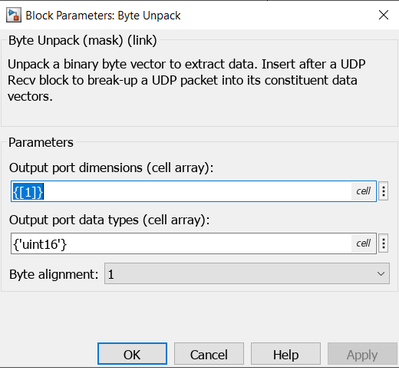
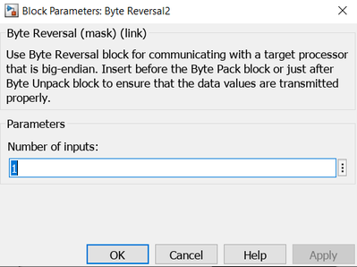
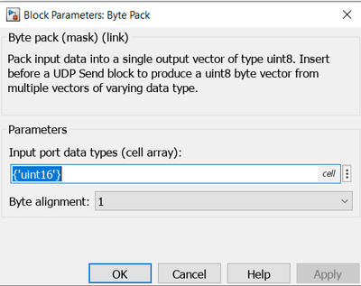
To obtain the reversed value, you will need another Data Store Memory and the Byte Unpack, Byte Reversal and the Byte Pack blocks.
They have to be configured as follows:
The Data Store Memory that will hold the reversed data has to be set up similarly to the original Data Store Memory block, same array initialization, same data type.
Byte Unpack receives 2 uint8 values and transforms them into a uint16 value.
The Byte Reversal block only needs to have the number of inputs configured. This changes the order of the bytes in the variable.
For example
11001000 01110011 -> Byte Reversal -> 01110011 11001000
Byte Pack has to be configured to accept uint16 as input.
After that, you will be able to see the initial bytes in FreeMASTER after adding the variable to the Variable Watch section.
This newly obtained Data Store Read variable can also be used as an input for the SPI, sending the bytes in a different order.
Regards,
Robert V


