- Forums
- Product Forums
- General Purpose MicrocontrollersGeneral Purpose Microcontrollers
- i.MX Forumsi.MX Forums
- QorIQ Processing PlatformsQorIQ Processing Platforms
- Identification and SecurityIdentification and Security
- Power ManagementPower Management
- Wireless ConnectivityWireless Connectivity
- RFID / NFCRFID / NFC
- MCX Microcontrollers
- S32G
- S32K
- S32V
- MPC5xxx
- Other NXP Products
- S12 / MagniV Microcontrollers
- Powertrain and Electrification Analog Drivers
- Sensors
- Vybrid Processors
- Digital Signal Controllers
- 8-bit Microcontrollers
- ColdFire/68K Microcontrollers and Processors
- PowerQUICC Processors
- OSBDM and TBDML
- S32M
-
- Solution Forums
- Software Forums
- MCUXpresso Software and ToolsMCUXpresso Software and Tools
- CodeWarriorCodeWarrior
- MQX Software SolutionsMQX Software Solutions
- Model-Based Design Toolbox (MBDT)Model-Based Design Toolbox (MBDT)
- FreeMASTER
- eIQ Machine Learning Software
- Embedded Software and Tools Clinic
- S32 SDK
- S32 Design Studio
- GUI Guider
- Zephyr Project
- Voice Technology
- Application Software Packs
- Secure Provisioning SDK (SPSDK)
- Processor Expert Software
-
- Topics
- Mobile Robotics - Drones and RoversMobile Robotics - Drones and Rovers
- NXP Training ContentNXP Training Content
- University ProgramsUniversity Programs
- Rapid IoT
- NXP Designs
- SafeAssure-Community
- OSS Security & Maintenance
- Using Our Community
-
- Cloud Lab Forums
-
- Knowledge Bases
- ARM Microcontrollers
- i.MX Processors
- Identification and Security
- Model-Based Design Toolbox (MBDT)
- QorIQ Processing Platforms
- S32 Automotive Processing Platform
- Wireless Connectivity
- CodeWarrior
- MCUXpresso Suite of Software and Tools
- MQX Software Solutions
- RFID / NFC
-
- Home
- :
- Product Forums
- :
- MPC5xxx
- :
- Re: MPC5748G Flash Memory Remap
MPC5748G Flash Memory Remap
- Subscribe to RSS Feed
- Mark Topic as New
- Mark Topic as Read
- Float this Topic for Current User
- Bookmark
- Subscribe
- Mute
- Printer Friendly Page
- Mark as New
- Bookmark
- Subscribe
- Mute
- Subscribe to RSS Feed
- Permalink
- Report Inappropriate Content
Hello.
I am working on a bootloader for DEVKIT-MPC5748G,
and have successfully implemented flash memory erase and program operations,
as well as starting the application firmware.
Now I would like to utilize flash memory remap options
in order to be able to have two memory "slots" for application firmware.
That way I can swap between them when I need to update and run new firmware.
I couldn't find any code examples for this, so I wrote it on my own
by looking at the Flash Memory Controller (PFLASH) section in the MCU's reference manual.
However, I can't seem to get the memory remap to work.
I tried to remap 2MB of memory at logical address 0x01000000 to physical address 0x01200000.
I also tried it with 256KB with the same addresses, which didn't work either.
Here's my source code:
// Initializes the flash remap.
static void bootFlashRemapInit()
{
    // Setup the remap logic and physical addresses,
    // per-master enable, and region size.
    PFLASH.PFCRD[0].Word0.R = 0x01200000;
    PFLASH.PFCRD[0].Word1.R = 0x01000000;
    PFLASH.PFCRD[0].Word2.R = 0xffff0015;

    // Enable remap descriptor 0.
    PFLASH.PFCRDE.R = 0xffff0000;

    // Enable instruction remap.
    PFLASH.PFCRCR.B.IRMEN = 1;
}

// Enables the flash remap.
static void bootFlashRemapEnable()
{
    PFLASH.PFCRCR.B.GRMEN = 1;
}

// Disables the flash remap.
static void bootFlashRemapDisable()
{
    PFLASH.PFCRCR.B.GRMEN = 0;
}
Obviously, I call bootFlashRemapInit to initialize the remap, and bootFlashRemapEnable to enable it.
I found out in the errata for my chip mask (https://www.nxp.com/docs/en/errata/MPC5748G_0N78S.pdf)
that this chip has a known problem when trying to remap flash memory in address range 0x00F90000-0x00FBFFFF.
This is not the address range I am working with,
but it got me thinking that there might be problems with the flash addresses I am working with as well.
Does anybody have an idea of what the problem might be?
Are there errors in my source code, or could the chip itself have an error?
Thanks in advance!
Solved! Go to Solution.
- Mark as New
- Bookmark
- Subscribe
- Mute
- Subscribe to RSS Feed
- Permalink
- Report Inappropriate Content
Hi,
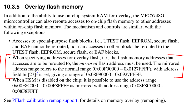
there's important note in the reference manual:

That means you should use mirrored address like this:
PFLASH.PFCRD[0].Word0.R = 0x09200000;
PFLASH.PFCRD[0].Word1.R = 0x01000000;
Then you will see content of address 0x01000000 at address 0x09200000 (not at 0x01200000 - this remains unchanged). The rest of your initialization seems to be correct.
Regards,
Lukas
- Mark as New
- Bookmark
- Subscribe
- Mute
- Subscribe to RSS Feed
- Permalink
- Report Inappropriate Content
Hi,
there's important note in the reference manual:

That means you should use mirrored address like this:
PFLASH.PFCRD[0].Word0.R = 0x09200000;
PFLASH.PFCRD[0].Word1.R = 0x01000000;
Then you will see content of address 0x01000000 at address 0x09200000 (not at 0x01200000 - this remains unchanged). The rest of your initialization seems to be correct.
Regards,
Lukas
- Mark as New
- Bookmark
- Subscribe
- Mute
- Subscribe to RSS Feed
- Permalink
- Report Inappropriate Content
Hey Lukas, thank you very much for answering! I definitely overlooked this.
However, this still didn't solve my problem. The remap is still not working, I'm simply always accessing the original location and not the remapped one.
In the meantime, I made a small test program in S32 Design Studio for Power Architecture, for MPC5748G, which has two functions that blink different LEDs, and are placed at two distinct memory locations.
Here's the source code:
#include "derivative.h" /* include peripheral declarations */
#define PA10 10
#define PA7 7extern void xcptn_xmpl(void);
__attribute__ ((section(".text1"))) void blink1()
{
uint32_t i;// Initialize DS4 LED.
SIUL2.MSCR[PA10].B.SSS = 0;
SIUL2.MSCR[PA10].B.OBE = 1;
SIUL2.MSCR[PA10].B.IBE = 0;
SIUL2.GPDO[PA10].B.PDO_4n = 1;while (1)
{
for (i = 0; i < 100000; i++);
// Blink DS4 LED.
SIUL2.GPDO[PA10].B.PDO_4n = !SIUL2.GPDO[PA10].B.PDO_4n;
}
}__attribute__ ((section(".text2"))) void blink2()
{
uint32_t i;// Initialize DS5 LED.
SIUL2.MSCR[PA7].B.SSS = 0;
SIUL2.MSCR[PA7].B.OBE = 1;
SIUL2.MSCR[PA7].B.IBE = 0;
SIUL2.GPDO[PA7].B.PDO_4n = 1;while (1)
{
for (i = 0; i < 100000; i++);
// Blink DS5 LED.
SIUL2.GPDO[PA7].B.PDO_4n = !SIUL2.GPDO[PA7].B.PDO_4n;
}
}int main(void)
{
// Configure and enable interrupts.
xcptn_xmpl();// Setup the remap logic and physical addresses,
// per-master enable, and region size.
PFLASH.PFCRD[0].Word0.R = 0x09100000; // logical address
PFLASH.PFCRD[0].Word1.R = 0x01200000; // physical address
PFLASH.PFCRD[0].Word2.R = 0xffff0012; // 256KB region// Enable remap descriptor 0.
PFLASH.PFCRDE.R = 0xffff0000;// Enable instruction remap.
PFLASH.PFCRCR.B.IRMEN = 1;// Enable flash remap.
PFLASH.PFCRCR.B.GRMEN = 1;blink1();
blink2(); // Won't be called but placed here so it would be included in the output file.while (1);
}
I also added the needed program sections to the flash linker file
...
MEMORY
{flash_rchw : org = 0x00FA0000, len = 0x4
cpu0_reset_vec : org = 0x00FA0000+0x10, len = 0x4
cpu1_reset_vec : org = 0x00FA0000+0x14, len = 0x4
cpu2_reset_vec : org = 0x00FA0000+0x04, len = 0x4
m_text : org = 0x01000000, len = 256K
m_text1 : org = 0x01100000, len = 256K
m_text2 : org = 0x01200000, len = 256K
m_data : org = 0x40000000, len = 768K
}...
.text1 :
{
*(.text1)
} > m_text1
.text2 :
{
*(.text2)
} > m_text2...
I've checked the generated .srec file, and the functions are indeed placed at the desired locations.
If I've understood it correctly, this code should call the blink2 function instead of blink1, since the memory has been remapped so that logical address 0x01100000 will point to the physical address 0x01200000. It still doesn't work, and always calls the blink1 function. I've tried setting the 27th bit (e.g. 0x09100000) in both the logical and physical addresses on or off, but none of the combinations work. And it's not that the execution will jump to an unprogrammed area in the flash memory, it just always accesses the original, unmapped location of 0x01100000.
Can you see any problems in this example? Maybe something else I forgot to initialize?
Thank you very much for your time.
- Mark as New
- Bookmark
- Subscribe
- Mute
- Subscribe to RSS Feed
- Permalink
- Report Inappropriate Content
Hi,
as I wrote, the remapping is visible only in mirrored flash address space. Normal address space remains unchanged after remapping. That means your code must be compiled to execute from mirrored flash address space (if it is not position independent code). And that also means you can't execute that code from normal address space.
Because there were more questions about this, I shared simple example here to show effect of the remapping:
https://community.nxp.com/docs/DOC-342943
Regards,
Lukas
- Mark as New
- Bookmark
- Subscribe
- Mute
- Subscribe to RSS Feed
- Permalink
- Report Inappropriate Content
Hey Lukas, thank you very much, again!
Sorry I didn't answer earlier, I couldn't return to working on this problem until recently.
Now I've done exactly as you said, compiling the code to execute from the mirrored flash address space,
and it works like a charm!
Thanks for all your help! You've saved me a lot of time and probably spared me a lot of frustration. :smileyhappy:
- Mark as New
- Bookmark
- Subscribe
- Mute
- Subscribe to RSS Feed
- Permalink
- Report Inappropriate Content
May I know how to compile the code to execute from the mirrored flash address space? What does it actually mean?