
- NXP Forums
- Product Forums
- General Purpose MicrocontrollersGeneral Purpose Microcontrollers
- i.MX Forumsi.MX Forums
- QorIQ Processing PlatformsQorIQ Processing Platforms
- Identification and SecurityIdentification and Security
- Power ManagementPower Management
- MCX Microcontrollers
- S32G
- S32K
- S32V
- MPC5xxx
- Other NXP Products
- Wireless Connectivity
- S12 / MagniV Microcontrollers
- Powertrain and Electrification Analog Drivers
- Sensors
- Vybrid Processors
- Digital Signal Controllers
- 8-bit Microcontrollers
- ColdFire/68K Microcontrollers and Processors
- PowerQUICC Processors
- OSBDM and TBDML
-
- Solution Forums
- Software Forums
- MCUXpresso Software and ToolsMCUXpresso Software and Tools
- CodeWarriorCodeWarrior
- MQX Software SolutionsMQX Software Solutions
- Model-Based Design Toolbox (MBDT)Model-Based Design Toolbox (MBDT)
- FreeMASTER
- eIQ Machine Learning Software
- Embedded Software and Tools Clinic
- S32 SDK
- S32 Design Studio
- Vigiles
- GUI Guider
- Zephyr Project
- Voice Technology
- Application Software Packs
- Secure Provisioning SDK (SPSDK)
- Processor Expert Software
-
- Topics
- Mobile Robotics - Drones and RoversMobile Robotics - Drones and Rovers
- NXP Training ContentNXP Training Content
- University ProgramsUniversity Programs
- Rapid IoT
- NXP Designs
- SafeAssure-Community
- OSS Security & Maintenance
- Using Our Community
-
- Cloud Lab Forums
-
- Home
- :
- QorIQ Processing Platforms
- :
- Layerscape
- :
- LS1046 Power Problem During PORESET_B de-assertion
LS1046 Power Problem During PORESET_B de-assertion
- Subscribe to RSS Feed
- Mark Topic as New
- Mark Topic as Read
- Float this Topic for Current User
- Bookmark
- Subscribe
- Mute
- Printer Friendly Page
LS1046 Power Problem During PORESET_B de-assertion
- Mark as New
- Bookmark
- Subscribe
- Mute
- Subscribe to RSS Feed
- Permalink
- Report Inappropriate Content
Hey,
I have a custom LS1046A board, which is heavily based off of the FRWY-LS1046 board, and I'm having some strange power behavior with my device.
1. First, even though I copied how the FRWY-LS1046 connects up the DIP switch for "cfg_rcw_src[0:8]", it seems to me that the device samples and saves these pins in reverse order into its registers. In other words, when I set the switches to the hard-coded setting "0x9F" or 0b0_1001_1111 on my DIP switch, the board does not go into "Hard-coded rcw" setting. But when I reverse the pins, e.g. 0x1F2 (0xF9 << 1), e.g. 0b1_1111_0010, then it does seem to enter "hard-coded rcw" setting. The device draws much more power, and this is also seen on the FRWY-LS1046 as well. Is this something that's already been observed by other users?
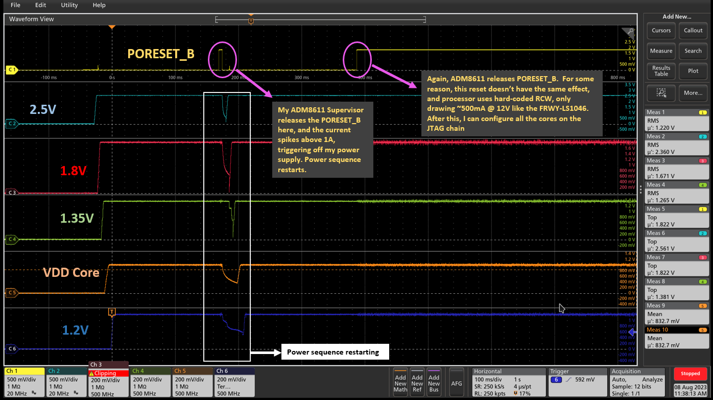
2. When I start is up in the "hard-coded rcw" setting, the current draw reaches ~1A @ 12V, and it is not able to connect on the JTAG chain. I've already described in a previous post that I can read from the processor's registers, so I don't think it's my JTAG interface. However, I can configure the JTAG chain when I do the following: if I set my power supply to have a current limit <1A @ 12V, then the power supply trips during boot up, and after it resets, the device goes through it's power sequence once again, and then the processor actually settles around 500mA @ 12V. When it does this, I can then see all the cores on the JTAG chain (shown in CCS log "nxp_question_01_success..._reset.txt")
This behavior is shown in the picture attached, "nxp_q02_power_reset.png", which shows the complete power sequence from t=0 to when the trip and reset happens, with descriptions on the signals. This test shown was done with the DIP switch in the proposed "0x1F2" configuration as mentioned above (putting the DIP switch at the expected 0x9F keeps current draw at 250mA @12V and doesn't get recognized by JTAG chain).
I still can't program the device correctly because the "reset_to_debug" CCS command makes the power supply trip again, as the devices tries to pull too much current. So my question is this: what could be pulling that much current at startup, which doesn't allow my processor to be found on the JTAG? And why does it work after this weird brownout condition?
I must've missed something, or incorrectly wired something in my design, but I have no idea what that could be, or where to look, as I've looked at various aspects of my board and can't find anything obvious yet.
Happy to provide any additional information
NOTE: the time scale on my oscope picture is 100ms/div, so even though the power sequence might not look quite right, I've got decent measurements that align with LS1046A Datasheet power-up sequence requirements.
Thanks,
-Nate J
- Mark as New
- Bookmark
- Subscribe
- Mute
- Subscribe to RSS Feed
- Permalink
- Report Inappropriate Content
Hello NFJ,
My team is attempting to boot a custom LS1046 board as well and we are in a similar situation.
We set our rcw source to QPSI.
On power up we sometimes read RCW + PBI commands from QSPI and boot.
More times than not we only read RCW and enter a bad state.
In the bad state RESET_REQ is asserted about 5 seconds after boot and we pull roughly 9A from the 1V rail.
On successful boots we pull about 1A on the 1V rail.
We've spent much time on this and your symptoms match ours.
Should we start an emotional support group?
- Mark as New
- Bookmark
- Subscribe
- Mute
- Subscribe to RSS Feed
- Permalink
- Report Inappropriate Content
Hey @AlexFromAmerica ,
An emotional support group sounds nice, haha
You might even be farther along than I am, as I haven't been able to program my QSPI flash since I can't connect to it fully with the JTAG.
Have you tried booting with the config_source pins in "Hard-coded RCW" mode? I'm interested to see if we get similar results in that way too.
Thanks,
-Nate
- Mark as New
- Bookmark
- Subscribe
- Mute
- Subscribe to RSS Feed
- Permalink
- Report Inappropriate Content
We generated an RCW+PBI using the QSCV process expert menus. This same RCW+PBI works on the RDB board.
Details about our design:
QSPI boot
Differential sys clock only (no single ended sys clock, no ddr clock).
- Mark as New
- Bookmark
- Subscribe
- Mute
- Subscribe to RSS Feed
- Permalink
- Report Inappropriate Content
I just suspect that it's in high-impendence during the PORESET_B. When the LS1046A is released from the reset status, the ASLEEP will be driven by the LS1046A.
Maybe you create a new case in the https://support.nxp.com/s/?language=en_US , press "Create New Case" button and send the schematics related to boot up part to us.
- Mark as New
- Bookmark
- Subscribe
- Mute
- Subscribe to RSS Feed
- Permalink
- Report Inappropriate Content
See attached waveform for HARDCODE boot mode of LS1046ARDB.
HARDCODE-FULL for the full sequence for the hardcode boot mode.
When PORESET in low voltage, ASLEEP is about 1.5V. It's high voltage is 1.8V(HARDCODE-ASLEEP).
When the PORESET fall, the ASLEEP nearly change at the same time(PORESET_FALL), when the PORESET is low, the ASLEEP won't change(PORESET_FALL_RISE). Why the ASLEEP pin will changed from low to 1.5V when PORESET assert in your board? I think the LS1046 should be in same status when PORESET assert. Please check why this pin will change?
And the FRWY1046 HARDCODE boot mode sequence looks different from the LS1046ARDB.
- Mark as New
- Bookmark
- Subscribe
- Mute
- Subscribe to RSS Feed
- Permalink
- Report Inappropriate Content
Hey @June_Lu ,
Edited: Additionally, I'd like to point out that in 3/4 of the four screenshots you sent in the post above, the ASLEEP pin only reaches 1.5V - all except for "HARDCODE_ASLEEP.png". It seems like 1.5V for ASLEEP is the nominal high voltage during PORESET_B, but "HARDCODE_ASLEEP.png" does indeed show it going up to 1.8V - why is that?
I apologize for taking so long to get back to you. I did verify that I am seeing 1.5V on the FRWY board, and the reset sequence is consistent when I look at it on the FRWY board.
Is it possible to get in touch with a team of NXP engineers to review my schematics?
My schematics are sensitive information, so I can't release them on this forum
Thanks,
-Nate J
- Mark as New
- Bookmark
- Subscribe
- Mute
- Subscribe to RSS Feed
- Permalink
- Report Inappropriate Content
I have checked your waveform and tested the same signals in my LS1046ARDB, why the high voltage of ASLEEP in the FRWY and your board both is 1.5V, I tested it about 1.8V. Could you double check it?
- Mark as New
- Bookmark
- Subscribe
- Mute
- Subscribe to RSS Feed
- Permalink
- Report Inappropriate Content
Hey @June_Lu ,
I did double check the ASLEEP pin on both boards, and I'm still seeing the same 1.5V result. I'm specifically probing the "CPU_ASLEEP" net, which is pin 2 of Q4 on the LS1046-FRWY board. Are you able to check this net on a FRWY board?
I noticed that the LS1046ARDB has a different MOSFET that it uses for the ASLEEP function - maybe that's why the gate voltage is staying high at 1.8V?
Thanks,
-Nate J
- Mark as New
- Bookmark
- Subscribe
- Mute
- Subscribe to RSS Feed
- Permalink
- Report Inappropriate Content
But the FRWY-LS1046 board seems load RCW from the attached capture in the green box, please confirm the SW1[1:9] = 0_1001_1110: Hard-coded RCW.
Please check the POR signals with oscilloscope at the rising edge of PORESET, including the PORESET rising time(including all signals in the LS1046A Reference Manual page 211). Make sure all meet the requirement.
Maximum rise/fall time of PORESET_B/HRESET_B refer LS1046A, LS1026A Data Sheet Table 23.
From the 1EE_0000h POR status register 1 (PORSR1) in the log(02_custom-board_ccs_read_rcw), it has recorded the RCW_SRC is 0x9F, it seems correct.
I think you could check if all signals related to PORESET are reliable for every power on, then set the LS1046 to reliable status.
Maybe you could send the schematics related to PORESET to review.
- Mark as New
- Bookmark
- Subscribe
- Mute
- Subscribe to RSS Feed
- Permalink
- Report Inappropriate Content
Hey @June_Lu ,
I checked the setup/hold times of the POR signals, and they all look to satisfy the requirements from the LS1046 datasheet. I attached a picture "custom-board-dip_001_annotated.png" that showcases one of my DIP switch pins on my custom board, and the setup (min. 4 SYSCLKS) & hold (min. 2 SYSCLKS), as well as rise time of my PORESET_B look to be satisfied.
What's the best way to submit my schematics to the NXP team? I can't post them on the forum, so is there a support page you can point me to, or help me send these schematics so that I can share them with you all?
Thanks,
-Nate J
- Mark as New
- Bookmark
- Subscribe
- Mute
- Subscribe to RSS Feed
- Permalink
- Report Inappropriate Content
Both the FRWY-LS1046 and customer board are the same boot mode? e.g., Hard-code mode? Same boot mode will be easy to compare each other. The AN12081 has Timing diagram of Boot process (Fig 4 or Fig 11). Please compare the difference between the FRWY-LS1046 and customer board. According to the voltage of respective signals in different steps, you will know which step is wrong.
"I'm guessing that maybe my POR signals aren't being read correctly during the first reset with no current limit, and for some reason that's putting the processor into a bad state? Not sure what to look for next. "
Please check the POR signals with oscilloscope at the rising edge of PORESET, including the PORESET rising time(including all signals in the LS1046A Reference Manual page 211). Make sure all meet the requirement. Especially the signals before the wrong step. It's better assess all the 4.4.1 Power-on reset sequence in the LS1046A Reference Manual.
- Mark as New
- Bookmark
- Subscribe
- Mute
- Subscribe to RSS Feed
- Permalink
- Report Inappropriate Content
Hey @June_Lu ,
Yes, both boards were in the same hard-coded mode. I have compared the differences in the photos provided on my previous reply. In each picture, I added a green box on the top that denotes what the captured oscilloscope image is displaying (my custom board or the FRWY-LS1046 board)
I have looked at the POR config pins, and they look as expected, with more than enough setup and hold time on them.
Are there any other pins I should try probing that might be worth looking at on the oscilloscope?
Thanks,
-Nate J
- Mark as New
- Bookmark
- Subscribe
- Mute
- Subscribe to RSS Feed
- Permalink
- Report Inappropriate Content
If you have checked the power supply meet the requirement of the LS1046A SPEC, please confirm the steps below:
- Have you disconnect RESET_REQ_B from PORESET_B( disconnect the J14 in the FRWY-LS1046). It is recommended to disconnect RESET_REQ_B from PORESET_B when using hard-coded RCW as any different board configuration may push the chip to an endless reset loop. For more information, see the hard-coded RCW options listed in QorIQ LS1046A Reference Manual (document LS1046ARM).
- Please try to check status of PORESET_B, HRESET_B, RESET_REQ_B, ASLEEP priority, check which boot process you are in. Please confirm the ASLEEP is low, then you will get into Hard coded RCW loads. Please confim all the signals could follow the AN12081 page 13 Timing diagram of RAM Boot process. AN12081: RAM Boot using CodeWarrior on LS1046ARDB Application Note
- If you could connect the JTAG successful and reliable(confirm the step 2 signals are correctly), check if the HARD-CODE bits could be written to the DCFG_CCSR_RCWSRx successfully. The steps could follow AN12081 "RAM boot process using CodeWarrior". The registers are shown in page 42.
- Mark as New
- Bookmark
- Subscribe
- Mute
- Subscribe to RSS Feed
- Permalink
- Report Inappropriate Content
Hey @June_Lu ,
Thank you for your reply. I looked at the signals you suggested, and have taken some measurements that I have attached to this reply.
With respect to your responses:
1. I have indeed disconnected RESET_REQ_B from PORESET_B (I included it in the oscilloscope images, but it is not actually resetting the device)
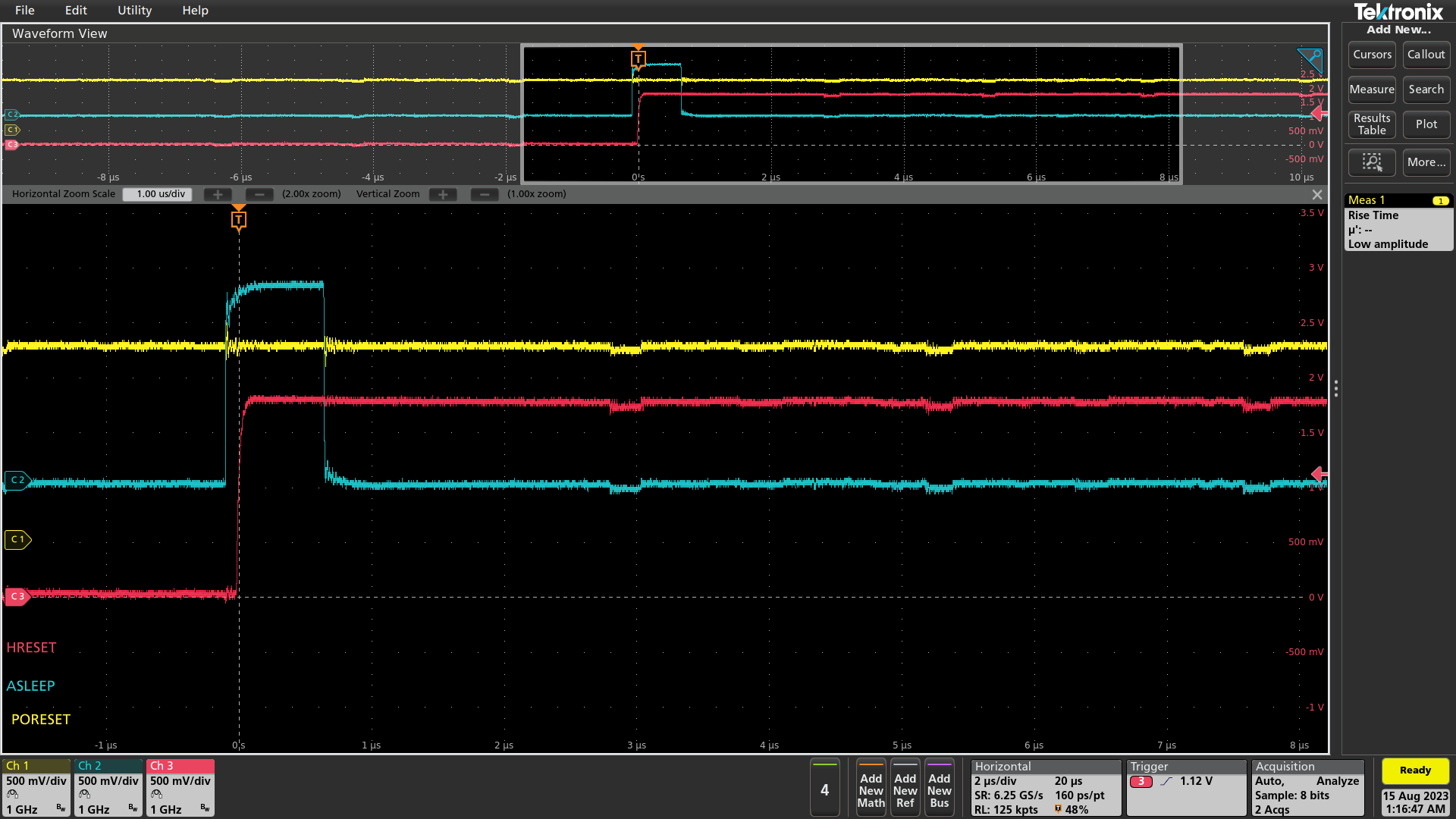
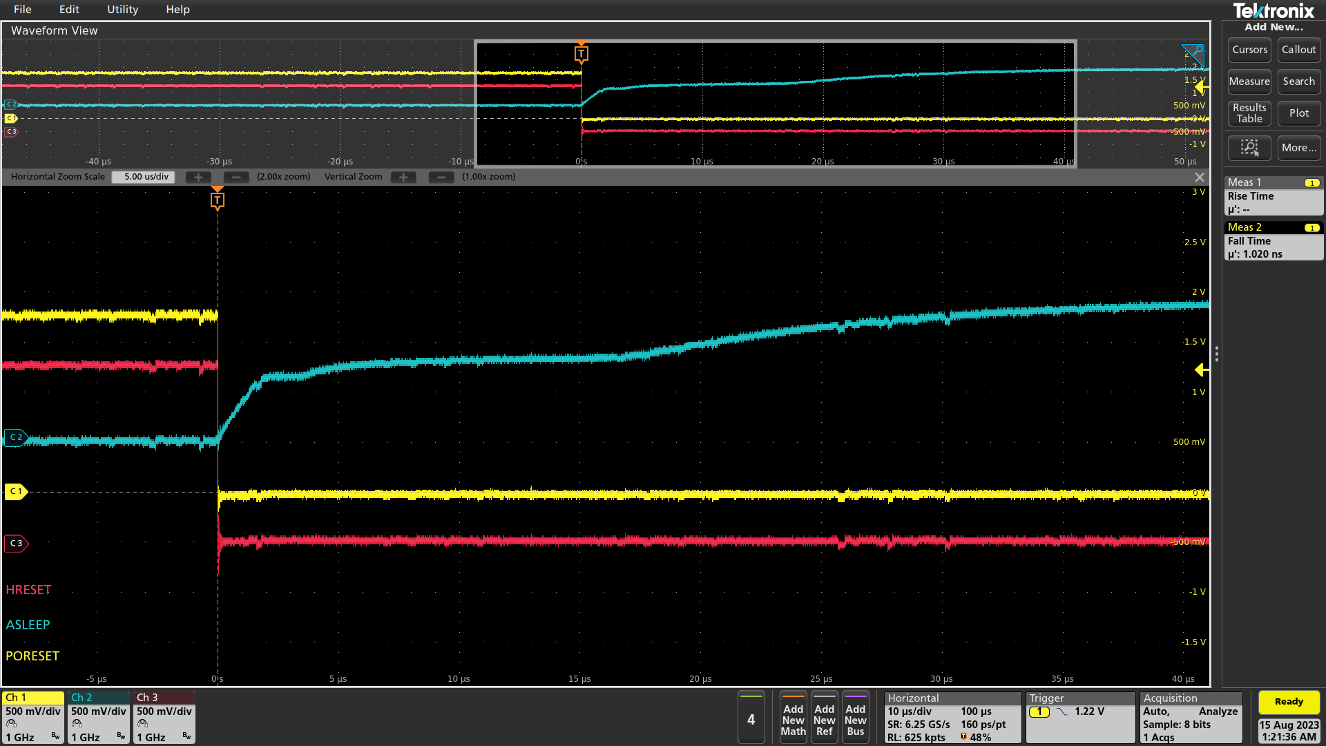
2. I have attached three attachments showing the differences between the FRWY-LS1046 board and my custom board. The detail of the images are as follows:
a. "FRWY-LS1046_power-on_..._-limit.png" is the result of the reset signals on the LS1046 that I measured on my oscilloscope. There is some noise on the ASLEEP pin, but that's probably due to my subpar soldering job
b. "custom-board_power-on_..._current-limit.png" shows what happens when I put a ~800mA current limit on my power supply. As previously shown, the device resets because the power supply momentarily shuts off, and then the device (for some reason) comes out of reset into an operational state where I can see all the cores on the JTAG.
c. "custom-board_power-on_..._no-current-limit.png" shows the result of the powering on of my board, with a much higher current limit. The board pulls around 1A, and it not reachable on the JTAG chain.
As you can see from the pictures, the FRWY board is definitely doing some extra work, as the ASLEEP pin stays high for much longer than it does on my board, but I don't really know why.
3. I have seen the RCW values after the board does the "double reset" with the power supply current-limited (picture referenced in 2.b.), and the results are attached in "custom-board_ccs_read_rcw.png". I have read the registers through CCS, using some commands I found in various application notes and forum posts.
I'm guessing that maybe my POR signals aren't being read correctly during the first reset with no current limit, and for some reason that's putting the processor into a bad state? Not sure what to look for next.
Any help or advice is appreciated.
Thanks,
-Nate J
- Mark as New
- Bookmark
- Subscribe
- Mute
- Subscribe to RSS Feed
- Permalink
- Report Inappropriate Content