- Forums
- Product Forums
- General Purpose MicrocontrollersGeneral Purpose Microcontrollers
- i.MX Forumsi.MX Forums
- QorIQ Processing PlatformsQorIQ Processing Platforms
- Identification and SecurityIdentification and Security
- Power ManagementPower Management
- Wireless ConnectivityWireless Connectivity
- RFID / NFCRFID / NFC
- Advanced AnalogAdvanced Analog
- MCX Microcontrollers
- S32G
- S32K
- S32V
- MPC5xxx
- Other NXP Products
- S12 / MagniV Microcontrollers
- Powertrain and Electrification Analog Drivers
- Sensors
- Vybrid Processors
- Digital Signal Controllers
- 8-bit Microcontrollers
- ColdFire/68K Microcontrollers and Processors
- PowerQUICC Processors
- OSBDM and TBDML
- S32M
- S32Z/E
-
- Solution Forums
- Software Forums
- MCUXpresso Software and ToolsMCUXpresso Software and Tools
- CodeWarriorCodeWarrior
- MQX Software SolutionsMQX Software Solutions
- Model-Based Design Toolbox (MBDT)Model-Based Design Toolbox (MBDT)
- FreeMASTER
- eIQ Machine Learning Software
- Embedded Software and Tools Clinic
- S32 SDK
- S32 Design Studio
- GUI Guider
- Zephyr Project
- Voice Technology
- Application Software Packs
- Secure Provisioning SDK (SPSDK)
- Processor Expert Software
- Generative AI & LLMs
-
- Topics
- Mobile Robotics - Drones and RoversMobile Robotics - Drones and Rovers
- NXP Training ContentNXP Training Content
- University ProgramsUniversity Programs
- Rapid IoT
- NXP Designs
- SafeAssure-Community
- OSS Security & Maintenance
- Using Our Community
-
- Cloud Lab Forums
-
- Knowledge Bases
- ARM Microcontrollers
- i.MX Processors
- Identification and Security
- Model-Based Design Toolbox (MBDT)
- QorIQ Processing Platforms
- S32 Automotive Processing Platform
- Wireless Connectivity
- CodeWarrior
- MCUXpresso Suite of Software and Tools
- MQX Software Solutions
- RFID / NFC
- Advanced Analog
-
- NXP Tech Blogs
- Home
- :
- ARM Microcontrollers
- :
- LPC微控制器知识库
- :
- [LPC546xx]:How To Re-enable SWD After Disabled
[LPC546xx]:How To Re-enable SWD After Disabled
[LPC546xx]:How To Re-enable SWD After Disabled
[LPC546xx]:How To Re-enable SWD After Disabled
This article mainly introduces how to re-enable SWD after disabled.
1.Problem description
The Enhanced Code Read Protection (ECRP) of the LPC546xx series is used to configure different security levels for user programs. It is configured when the startup image file offset is 0x20 and is used in combination with OTP. Users of LPC546xx can disable SWD and ISP by configuring ECRP values.
Some users need to re-enable SWD after disabling SWD, you can use the J-link commander "unlock LPC5460x" command or re-enable SWD based on LPC-LINK2 CMSIS-DAP these two methods, this article will introduce the two methods in detail.
2.Theoretical analysis and solutions
Customer’s example:
LPC54605:Configure ECRP to 0x00015800. After disabling SWD, it needs to be restored.
When the ECRP value is 0x00015800, we analyze from high to low through user manual.
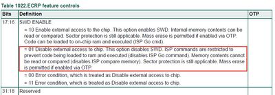
In ECRP, 31:18 bits are reserved, and 17:16 bits determine the status of SWD.
In this example, 17:16=01 ,this means that SWD is disabled.
15: 14 =01, it is not allowed to enter ISP through IAP call.
13: 12 = 01, it is not allowed to enter ISP through pin.
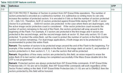
11: 10 = 10, IAP sector erase / write protection is disabled, so sector protect (5:0) is ignored.
At this point, SWD (17:16) is DISABLED, ISP Entry from ISP (15:14) is DISABLED, and ISP Entry from Bootloader (13:12) is DISABLED, the IAP Mass Erase can still be used to erase the entire Flash to recover a device. as long as the OTP MASS ERASE is ENABLED. If the OTP has been configured and bit 4 is set to 1, that is, disabled mass erase command, the SWD can never be recovered again.
When Mass Erase is enabled, the Debug Mailbox is also enabled and allows a debugger to communicate with the bootloader to execute a Mass Erase.
Therefore, the Debug Mailbox can be used to perform Mass Erase operation and restore ECRP settings. To achieve the purpose of re-enabling SWD.
3. Re-enable SWD
3.1 Use "unlock LPC5460x" command re-enable SWD
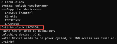
If use J-link debug probe, use "unlock LPC5460x" command to re-enable SWD.
- Open the J-Link commander and enter unlock to view supported devices.
- Enter the corresponding chip command. In this paper, the command is unlock LPC5460x.
As shown in the picture below:
However, for some chips, this method still fails to re-enable SWD. The following is a method of SWD recovery based on LPC-LINK2 CMSIS DAP. If the unlock LPC546xx command does not work, use the following method.
3.2 LPC-LINK2 CMSIS-DAP re-enable SWD
If use CMSIS-DAP debug probe, use below steps to re-enable SWD.
IDE: MCUXpresso IDE v11.7.1_9221 or other version.
IDE installation path: C:\nxp\ MCUXpresso IDE v11.7.1_9221.
The development board emulator firmware uses LPC-LINK2 CMSIS-DAP.
Tool script: LPC546xxMassErase.scp.
Tool script path: C:\nxp\ MCUXpresso IDE v11.7.1_9221 \ide\binaries\Scripts.
The operations are the same for other versions of MCUXpressoIDE and other installation paths.
1) Put LPC546xxMassErase.scp script in the path:
C:\nxp\MCUXpressoIDE_11.7.1_922\ide\binaries\Scripts
2) Open a command prompt window.
3) Change the path to C:\nxp\ MCUXpresso IDE v11.7.1_9221 \ide\binaries.
4) Run the redlinkserv -commandline command.
5) After running the redlinkserv -commandline command, you should see the redlink> prompt.
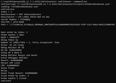
6) Run the load command "C:\nxp\MCUXpressoIDE_11.7.1_9221\ide\binaries\Scripts\LPC546xxMassErase.scp".
7) After executing the load command, you should see that "LPC546xxMassErase.scp" is being loaded.
9) After executing the run command, you should see the following message.
In this case, the SWD interface can be used normally.
4.Query ECRP level
In the LPC546xx user manual, we can see ISP-AP command, one function is query the ECRP level, that is, to view the ECRP configuration of this chip.
From the log in part 3, we can see the returned ECRP level:
However, there is no explanation in the user manual, so here we show the meanings of each bit.
There is a table translation from the ECRP level user defined and the ECRP definition used by the ROM code:
/* Feature bit defines */
#define CRP_JTAG_EN_BIT (1 << 6)
#define CRP_MASS_ERASE_DIS_BIT (1 << 7)
#define CRP_IAP_PROT_EN_BIT (1 <<
#define CRP_ISP_PINS_EN_BIT (1 << 9)
#define CRP_ISP_IAP_EN_BIT (1 << 10)
#define CRP_DBG_MBOX_EN_BIT (1 << 11)
#define CRP_COUNT_MASK 0x3F
#define CRP_DEFAULT_FEATURES 0xFFFFFFFF
#define CRP_MASS_ERASE_ONLY (CRP_SECT_ERASE_DIS_BIT)
For example:
In CRP_JTAG_EN_BIT, 1 is JTAG/SWD enabled and 0 is disabled. It’s corresponding to ECRP value bit 17 and 16.
In CRP_MASS_ERASE_DIS_BIT, 0 is Mass Erase allowed and 1 is disallowed. It’s corresponding to the combination of ECRP value bit 0~5, bit 10~11, and bit 14~15.
In CRP_IAP_PROT_EN_BIT, 1 is IAP protection enabled and 0 is disabled. It’s corresponding to ECRP value bit 14~15.
In CRP_ISP_PINS_EN_BIT, 1 is ISP pin enabled and 0 is disabled. It’s corresponding to ECRP value bit 12~13.
In CRP_ISP_IAP_EN_BIT, 1 is ISP in IAP mode enabled and 0 is disabled. It’s corresponding to ECRP value bit 14~15.
In CRP_DBG_MBOX_EN_BIT, 1 is ISP-AP or debugger mailbox enabled and 0 is disabled. It’s corresponding the combination of some reserved ECRP bits and OTP setting.
Of course, all these ECRP value used by the ROM not only look into the user defined ECRP value but also check the OTP setting. When “Query ECRP Level” is called, it returns the value used by the ROM code, but not the ECRP value programmed in the image by the user.
5.Summary:
In the LPC546xx series, even if SWD is disabled, the debugger can communicate with LPC5460x through the Debug mailbox. As long as OTP does not disable Mass Erase, the debugger can ask LPC5460x to perform mass erase through the Debug Mailbox to re-enable SWD functionality.
In addition, the article also adds the specific meaning of the value returned by the ISP-AP command.


