- Forums
- Product Forums
- General Purpose MicrocontrollersGeneral Purpose Microcontrollers
- i.MX Forumsi.MX Forums
- QorIQ Processing PlatformsQorIQ Processing Platforms
- Identification and SecurityIdentification and Security
- Power ManagementPower Management
- MCX Microcontrollers
- S32G
- S32K
- S32V
- MPC5xxx
- Other NXP Products
- Wireless Connectivity
- S12 / MagniV Microcontrollers
- Powertrain and Electrification Analog Drivers
- Sensors
- Vybrid Processors
- Digital Signal Controllers
- 8-bit Microcontrollers
- ColdFire/68K Microcontrollers and Processors
- PowerQUICC Processors
- OSBDM and TBDML
- S32M
-
- Solution Forums
- Software Forums
- MCUXpresso Software and ToolsMCUXpresso Software and Tools
- CodeWarriorCodeWarrior
- MQX Software SolutionsMQX Software Solutions
- Model-Based Design Toolbox (MBDT)Model-Based Design Toolbox (MBDT)
- FreeMASTER
- eIQ Machine Learning Software
- Embedded Software and Tools Clinic
- S32 SDK
- S32 Design Studio
- GUI Guider
- Zephyr Project
- Voice Technology
- Application Software Packs
- Secure Provisioning SDK (SPSDK)
- Processor Expert Software
- MCUXpresso Training Hub
-
- Topics
- Mobile Robotics - Drones and RoversMobile Robotics - Drones and Rovers
- NXP Training ContentNXP Training Content
- University ProgramsUniversity Programs
- Rapid IoT
- NXP Designs
- SafeAssure-Community
- OSS Security & Maintenance
- Using Our Community
-
- Cloud Lab Forums
-
- Knowledge Bases
- ARM Microcontrollers
- i.MX Processors
- Identification and Security
- Model-Based Design Toolbox (MBDT)
- QorIQ Processing Platforms
- S32 Automotive Processing Platform
- Wireless Connectivity
- CodeWarrior
- MCUXpresso Suite of Software and Tools
- MQX Software Solutions
-
- Home
- :
- ARM Microcontrollers
- :
- Kinetis微控制器知识库
- :
- Yes, OSDA can trim the reference of internal clock source!
Yes, OSDA can trim the reference of internal clock source!
Yes, OSDA can trim the reference of internal clock source!
Yes, OSDA can trim the reference of internal clock source!
Trimming internal reference clock of ICS (internal clock source) module using OSDA connection
Pavel Šádek, Rožnov, Czech Republic
Simple apps does not require crystal driven clock precision. Internal reference clock based timing of MCU can be used instead.
Manufacturing process yealds to frequency deviation, that is why all MCU devices are factory programmed with a trim value in a reserved memory location. This value is uploaded to the ICS_C3 register and ICS_C4[SCFTRIM] during any reset initialization. For finer precision, trim the internal oscillator in the application and set ICS_C4[SCFTRIM] accordingly.
The TRIM bits effect the ICSOUT frequency if the ICS is in FLL engaged internal (FEI), FLL bypassed internal (FBI), or FLL bypassed internal low power (FBILP) mode.
The internal reference clock can be trimmed also in program time of the device to any value between 31.25 and 39.062kHz, this allows also achieving exotic bus frequencies.
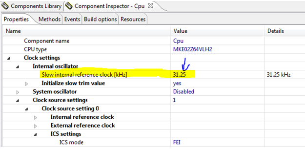
The value applied in Processor Expert does not propagate into Pemicro connection manager.
No matter if Processor expert is used or not , we need to configure it it by ourselves in connection of OSDA (same for debugging or programming). So this is a guide how to do so.
In the program initialization we need to initialize the ICS_C3 register and ICS_C4[SCFTRIM]. It can be done siply this way:
/* System clock initialization */
if ( *((uint8_t*) 0x03FFU) != 0xFFU) {
ICS_C3 = *((uint8_t*) 0x03FFU);
ICS_C4 = (ICS_C4 & 0xFEU) | ((*((uint8_t*) 0x03FEU)) & 0x01U);
}
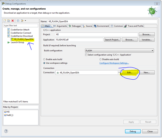
Then hit
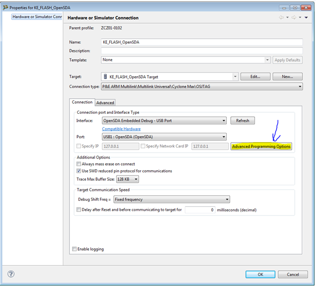
You will get new window
Choose „Advanced Programming Options“ button
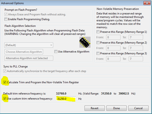
Enable calculating of Trim value and programming into Flash location.
If the TRIM frequency is different from default, check the box to use custom one in valid range – the one you(or Processor Expert) have used for your timing calculations.
Hit DONE and your effort is done!
Next, when you will launch debugging session by hitting bug on button 
My RESULT:
ICS_C3 was trimmed to value of
0x57 for 39.062kHz and
0x9B for 31.250kHz
for my Kinetis E Freedom board.
Precision is better then 1% in room temp. This is ok for serial comunication without need of crystal for example.
Note:
Values out from my discovered range of 0x57 – 0x9B leads to frequencies that are out of specification of ICS and should not be used for this exact device. The limits will be slightly different for every single device.
Can this be done with a USBDM or JLINK? Thanks.
Hi,
Thank you so much for sharing this. I have questions about this for KE04 series MCU :
1. Will the value trimmed by ourselves be stored in the flash or somewhere ? Where is the address ?
2. Will the value trimmed by ourselves be loaded to ICS_C3, C4 automatically ? If not, what/how we need to do ?
Thanks.
Best regards,
Stanley


