- 新着としてマーク
- ブックマーク
- 購読
- ミュート
- RSS フィードを購読する
- ハイライト
- 印刷
- 不適切なコンテンツを報告
I'm attempting to program a K81 and QSPI (Micron MT25QL128 - 16MB, single die). Segger J-Flash V7.54c shows error:
Timeout while preparing target, RAMCode did not respond in time. (PC = 0x00000000, CPSR = 0x00000000, LR = 0x61000000)!
Failed to prepare RAMCode using RAM
Error while determining flash info (Bank 1 @ 0x68000000)
Failed to auto program target
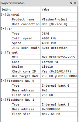
The J-Flash Project Info:
Has anyone encountered this, and can figure what's going on?
Thanks,
Denis
解決済! 解決策の投稿を見る。
- 新着としてマーク
- ブックマーク
- 購読
- ミュート
- RSS フィードを購読する
- ハイライト
- 印刷
- 不適切なコンテンツを報告
J-Flash/J-Link V6.50a works perfectly. There's a bug in V7.45c, which I have reported to Segger.
Update Jan 20, 2022 from Segger:
Upcoming release of Segger J-Link/J-Flash will include fix for this issue.
The issue was due to a speed optimization that relied on the availability of an external reference clock, RTCK, which is not the case with many devices, including the NXP K8x.
Update Jan 25, 2022:
Segger J-Link/J-Flash V7.60f available for download. Fix for K8x issue included in this release.
- 新着としてマーク
- ブックマーク
- 購読
- ミュート
- RSS フィードを購読する
- ハイライト
- 印刷
- 不適切なコンテンツを報告
Hi,
When you use jFlash, you doesn't configure the QSPI. So the external ram can't be used.
Have a great day,
-------------------------------------------------------------------------------
Note:
- If this post answers your question, please click the "Mark Correct" button. Thank you!
- We are following threads for 7 days after the last post, later replies are ignored
Please open a new thread and refer to the closed one, if you have a related question at a later point in time.
-------------------------------------------------------------------------------
- 新着としてマーク
- ブックマーク
- 購読
- ミュート
- RSS フィードを購読する
- ハイライト
- 印刷
- 不適切なコンテンツを報告
@nxf56274I'm not sure what you're saying. There is no external RAM, only the K81 with its onboard internal RAM.
As I understand the process, in order to write to the external QSPI flash, j-Flash/J-Link first downloads code to the MCU's internal RAM, sets the program counter and starts execution. Thereafter, J-Link/J-Flash sends instructions and data to the RAM resident code, which relays it to the external QSPI flash.
Thanks,
Denis
