- NXP Forums
- Product Forums
- General Purpose MicrocontrollersGeneral Purpose Microcontrollers
- i.MX Forumsi.MX Forums
- QorIQ Processing PlatformsQorIQ Processing Platforms
- Identification and SecurityIdentification and Security
- Power ManagementPower Management
- MCX Microcontrollers
- S32G
- S32K
- S32V
- MPC5xxx
- Other NXP Products
- Wireless Connectivity
- S12 / MagniV Microcontrollers
- Powertrain and Electrification Analog Drivers
- Sensors
- Vybrid Processors
- Digital Signal Controllers
- 8-bit Microcontrollers
- ColdFire/68K Microcontrollers and Processors
- PowerQUICC Processors
- OSBDM and TBDML
-
- Solution Forums
- Software Forums
- MCUXpresso Software and ToolsMCUXpresso Software and Tools
- CodeWarriorCodeWarrior
- MQX Software SolutionsMQX Software Solutions
- Model-Based Design Toolbox (MBDT)Model-Based Design Toolbox (MBDT)
- FreeMASTER
- eIQ Machine Learning Software
- Embedded Software and Tools Clinic
- S32 SDK
- S32 Design Studio
- Vigiles
- GUI Guider
- Zephyr Project
- Voice Technology
- Application Software Packs
- Secure Provisioning SDK (SPSDK)
- Processor Expert Software
-
- Topics
- Mobile Robotics - Drones and RoversMobile Robotics - Drones and Rovers
- NXP Training ContentNXP Training Content
- University ProgramsUniversity Programs
- Rapid IoT
- NXP Designs
- SafeAssure-Community
- OSS Security & Maintenance
- Using Our Community
-
- Cloud Lab Forums
-
- Home
- :
- General Purpose Microcontrollers
- :
- Kinetis Microcontrollers
- :
- Can't connect to K02 with USB Multilink
Can't connect to K02 with USB Multilink
- Subscribe to RSS Feed
- Mark Topic as New
- Mark Topic as Read
- Float this Topic for Current User
- Bookmark
- Subscribe
- Mute
- Printer Friendly Page
- Mark as New
- Bookmark
- Subscribe
- Mute
- Subscribe to RSS Feed
- Permalink
- Report Inappropriate Content
Hello
I already used the pemicro USB multilink with Kinetis K60 and K70 (On CodeWarior and KDS)
Now, I start a new project on a K02 with MCUXpresso.
But when I want start the debug, I get the following error (like if target not connected) Refer to the attached jpeg.
What I should check first? (Blue Led and Orange Led are well light on on the PE micro Multilink universal.
To resume, the IDE is new for me and the microcontroller is new for me. then It is not easy to determine if problem comes from the hardware or something into MCUXpresso..
Please find the hardware schematic.
Thank for your help.
Solved! Go to Solution.
- Mark as New
- Bookmark
- Subscribe
- Mute
- Subscribe to RSS Feed
- Permalink
- Report Inappropriate Content
Hello
It is an MK02FN64VLH10.
But I just found the problem, it was a short-circuit between TDO and TCLK.
But just a question, we link the JTAG Reset to the pin of MCU 'JTAG-RST' wichi is by defaut a gpio pin function.
Then Should we instead link the Jtag reset to the RESET pin of the MCU K02?
- Mark as New
- Bookmark
- Subscribe
- Mute
- Subscribe to RSS Feed
- Permalink
- Report Inappropriate Content
Hi,
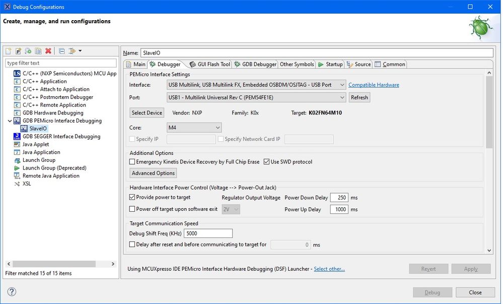
Following is that I use because it was I used in CW and KDS..
I don't now the 'LS' connection. How associate it to the Pemicro probe? It ask me a "LinkServer"??
-Then finally, what is the advantage of the SWD related to the JTAG?
-Is cyclone Fx has the SWD link? (used in production)
- Mark as New
- Bookmark
- Subscribe
- Mute
- Subscribe to RSS Feed
- Permalink
- Report Inappropriate Content
Hi Arnaud Girard,
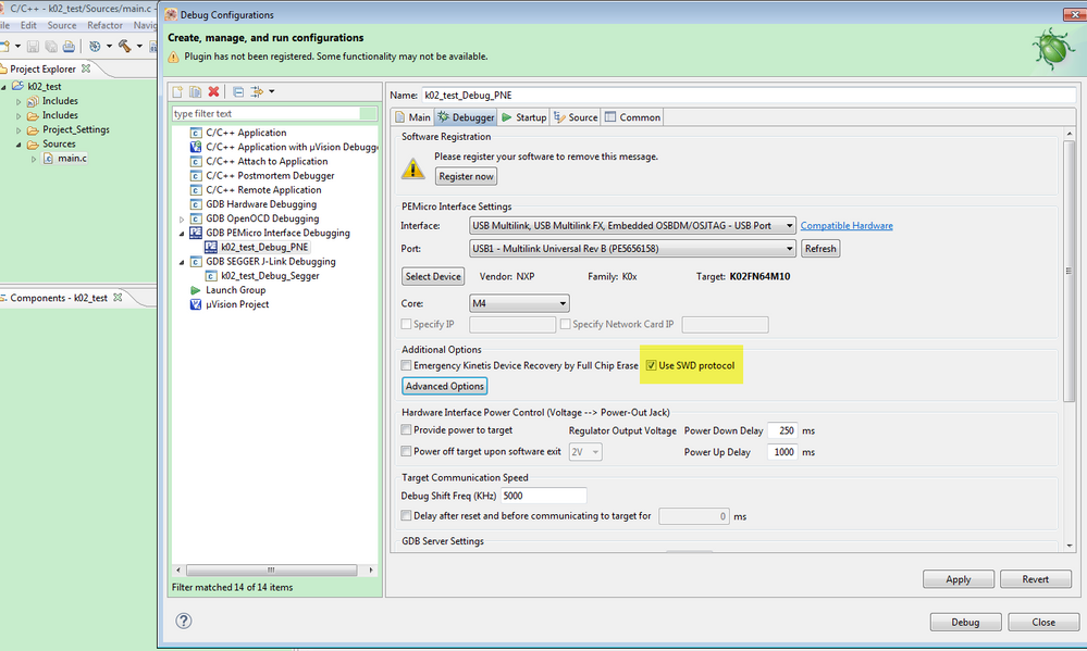
In fact, you are using the SWD interace in your code.
Your debugger can support the SWD.
Now, what's the debugger result?
Do you have Segger JLINK on your side? If yes, you can use the JLINK commander to connect your board at first, whether you can find the ARM core or not? If you can't find the ARM core, it means your hardware still have problems.
Have a great day,
Kerry
-------------------------------------------------------------------------------
Note:
- If this post answers your question, please click the "Mark Correct" button. Thank you!
- We are following threads for 7 weeks after the last post, later replies are ignored
Please open a new thread and refer to the closed one, if you have a related question at a later point in time.
-------------------------------------------------------------------------------
- Mark as New
- Bookmark
- Subscribe
- Mute
- Subscribe to RSS Feed
- Permalink
- Report Inappropriate Content
Hello,
I do not know this interface.
Is it is present on USB Multilink universal PortF used for Kinetis?
What is the difference on the using? On the MCUXpresso debugging interface?
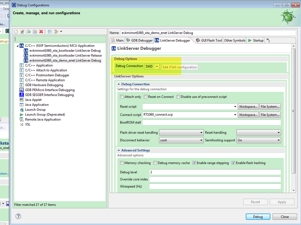
How configure MCUXpresso to switch from the JTAG to SWD?
- Mark as New
- Bookmark
- Subscribe
- Mute
- Subscribe to RSS Feed
- Permalink
- Report Inappropriate Content
Hi Arnaud Girard,
Multilink can support the SWD directly.
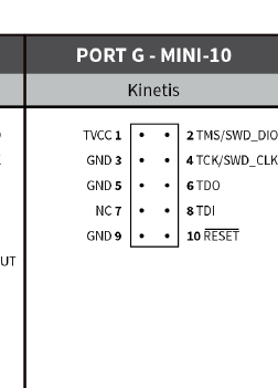
Other port is the same, you just need to use the SWD_DIO, SWD_CLK, RESET, VCC and GND.
Kinetis chip related pin: PTA3 is SWD_DIO, PTA0 is SWD_CLK. RESET is your MCU RESETB.
About the MCUXPresso IDE, do you modify the JTAG debugger interface? If not, it should in default using the SWD.
Have a great day,
Kerry
-------------------------------------------------------------------------------
Note:
- If this post answers your question, please click the "Mark Correct" button. Thank you!
- We are following threads for 7 weeks after the last post, later replies are ignored
Please open a new thread and refer to the closed one, if you have a related question at a later point in time.
-------------------------------------------------------------------------------
- Mark as New
- Bookmark
- Subscribe
- Mute
- Subscribe to RSS Feed
- Permalink
- Report Inappropriate Content
Hi Arnaud Girard ,
Please tell me your K02 chip full name, the part number, your schematic picture partnumber name also is not completed.
Please give me you chip partnumber, then I can help you to check more details.
Waiting for your updated information.
Have a great day,
Kerry
-------------------------------------------------------------------------------
Note:
- If this post answers your question, please click the "Mark Correct" button. Thank you!
- We are following threads for 7 weeks after the last post, later replies are ignored
Please open a new thread and refer to the closed one, if you have a related question at a later point in time.
-------------------------------------------------------------------------------
- Mark as New
- Bookmark
- Subscribe
- Mute
- Subscribe to RSS Feed
- Permalink
- Report Inappropriate Content
Hello
It is an MK02FN64VLH10.
But I just found the problem, it was a short-circuit between TDO and TCLK.
But just a question, we link the JTAG Reset to the pin of MCU 'JTAG-RST' wichi is by defaut a gpio pin function.
Then Should we instead link the Jtag reset to the RESET pin of the MCU K02?
- Mark as New
- Bookmark
- Subscribe
- Mute
- Subscribe to RSS Feed
- Permalink
- Report Inappropriate Content
Hi Arnaud Girard,
Thanks for your updated information.
Do you try the SWD interface instead of JTAG?
SWD_DIO is better to add external 10K pull up.
Reset_b pin need to add external 10K pull up and 0.1uf capacitor to ground.
About the reset, normally, we connect the MCU reset_b pin to the SWD interface.
It means, the SWD interface have these signals: SWD_DIO, SWD_CLK, RESET_b, VDD and GND.
Can you accept the SWD interface?
Have a great day,
Kerry
-------------------------------------------------------------------------------
Note:
- If this post answers your question, please click the "Mark Correct" button. Thank you!
- We are following threads for 7 weeks after the last post, later replies are ignored
Please open a new thread and refer to the closed one, if you have a related question at a later point in time.
-------------------------------------------------------------------------------


