- NXP Forums
- Product Forums
- General Purpose MicrocontrollersGeneral Purpose Microcontrollers
- i.MX Forumsi.MX Forums
- QorIQ Processing PlatformsQorIQ Processing Platforms
- Identification and SecurityIdentification and Security
- Power ManagementPower Management
- MCX Microcontrollers
- S32G
- S32K
- S32V
- MPC5xxx
- Other NXP Products
- Wireless Connectivity
- S12 / MagniV Microcontrollers
- Powertrain and Electrification Analog Drivers
- Sensors
- Vybrid Processors
- Digital Signal Controllers
- 8-bit Microcontrollers
- ColdFire/68K Microcontrollers and Processors
- PowerQUICC Processors
- OSBDM and TBDML
-
- Solution Forums
- Software Forums
- MCUXpresso Software and ToolsMCUXpresso Software and Tools
- CodeWarriorCodeWarrior
- MQX Software SolutionsMQX Software Solutions
- Model-Based Design Toolbox (MBDT)Model-Based Design Toolbox (MBDT)
- FreeMASTER
- eIQ Machine Learning Software
- Embedded Software and Tools Clinic
- S32 SDK
- S32 Design Studio
- Vigiles
- GUI Guider
- Zephyr Project
- Voice Technology
- Application Software Packs
- Secure Provisioning SDK (SPSDK)
- Processor Expert Software
-
- Topics
- Mobile Robotics - Drones and RoversMobile Robotics - Drones and Rovers
- NXP Training ContentNXP Training Content
- University ProgramsUniversity Programs
- Rapid IoT
- NXP Designs
- SafeAssure-Community
- OSS Security & Maintenance
- Using Our Community
-
- Cloud Lab Forums
-
- Home
- :
- General Purpose Microcontrollers
- :
- Kinetis Microcontrollers
- :
- SWD pin 30 with PWM/IO - MKE02Z16VLC4
SWD pin 30 with PWM/IO - MKE02Z16VLC4
- Subscribe to RSS Feed
- Mark Topic as New
- Mark Topic as Read
- Float this Topic for Current User
- Bookmark
- Subscribe
- Mute
- Printer Friendly Page
SWD pin 30 with PWM/IO - MKE02Z16VLC4
- Mark as New
- Bookmark
- Subscribe
- Mute
- Subscribe to RSS Feed
- Permalink
- Report Inappropriate Content
Hi, greetings.
What's wrong? How to I use FTM1_CH0 as PWM output?
(pin 30 = PTC4/RTCO/FTM1_CH0/ACMP0_IN2/SWD_CLK)
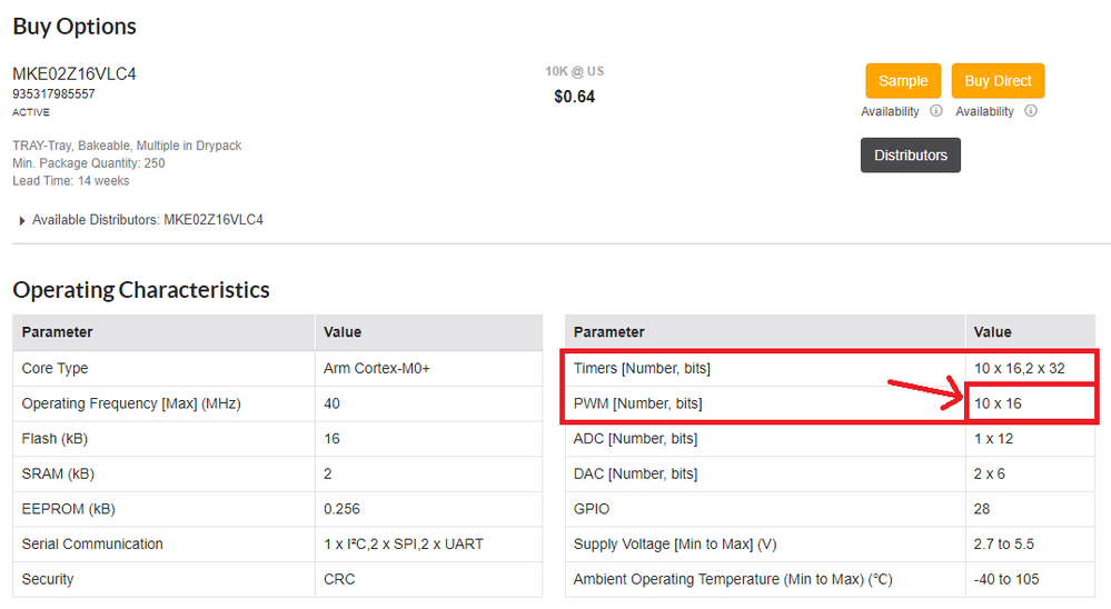
PWM[Number, bits] > 9 x 16?
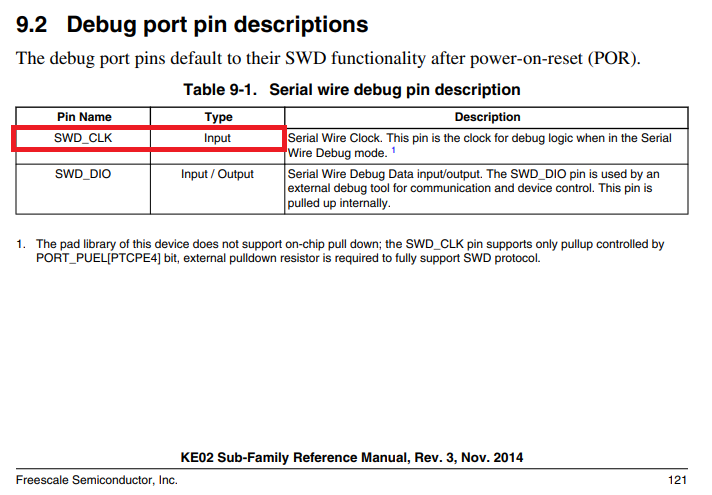
It is an only input pin, do not possible set to output PWM. I am wrong?
Thanks.
Tonn.
- Mark as New
- Bookmark
- Subscribe
- Mute
- Subscribe to RSS Feed
- Permalink
- Report Inappropriate Content
Hi, Sabina,
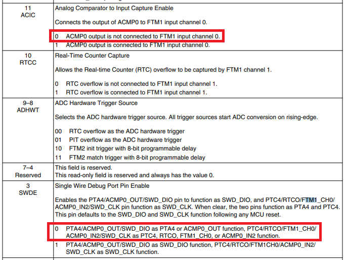
I'm sorry it was a misinterpretation of the datasheet made me doubt what I was doing, common when we read something technical in a language other than our daily lives. Not only, but I was also mistaken in thinking I was doing it the right way. In my case, I also did the bit mask incorrectly, now it's right, solved with these two lines:
SIM_SOPT &= ~SIM_SOPT_SWDE_MASK; //IO_map.h - clear bit SWDE now is right
SIM_SOPT &= ~SIM_SOPT_ACIC_MASK; //
Thank you very much.
Solved.
Daniel.
- Mark as New
- Bookmark
- Subscribe
- Mute
- Subscribe to RSS Feed
- Permalink
- Report Inappropriate Content
Hello Daniel,
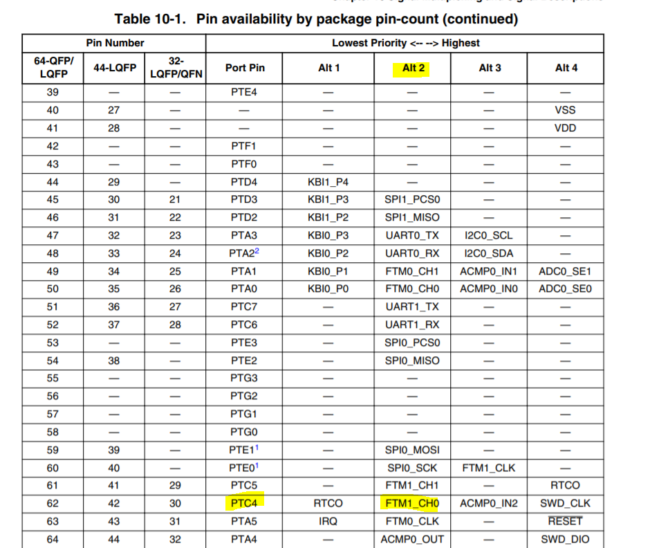
Pin 30, is the Pin 4 of the Port C register. You have to initialize it as the alternative function 2 in order to use it as the FTM1_CH0 as you mention above. You can see this in the table 10-1 of the user manual.
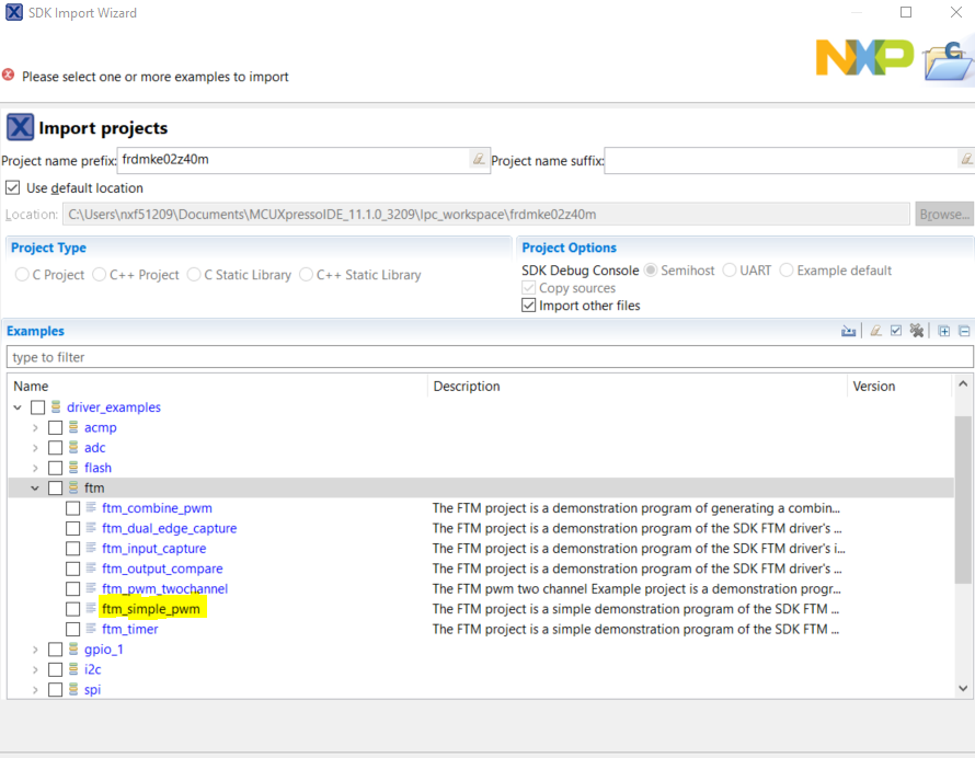
I would recommend to download our SDK for the FRDM-KE02Z. Once downloaded you can import the SDK examples. Here you will find several that use the FTM module for the different modes it has. As you can see there is one for creating a PWM signal. You may use this as a reference.
Please let me know if you have further questions.
Best Regards,
Sabina
- Mark as New
- Bookmark
- Subscribe
- Mute
- Subscribe to RSS Feed
- Permalink
- Report Inappropriate Content
Sabina, thanks for your response.
I want to use all outputs with PWM (ten). I'm using KDS IDE, processor expert for initializations.
After initialize program, guaranted disabled SWD pin functions in SIM_SOPT, bit 3. On program runing all pins responsed ok, howeder, FTM1_CH0 "thinking about life", no action.
In fact, this pin is input or output or all? Note: Capture mode, the pin = input, edge alined PWM mode = output...
Exists a equivalent schematic to specific I/O input in any tech document? I not ecountered, possibly wold understand better.
- Mark as New
- Bookmark
- Subscribe
- Mute
- Subscribe to RSS Feed
- Permalink
- Report Inappropriate Content
Hello Daniel,
The FTM1 signal description are as follows:
This means that it is possible to use it as input or output.
Make sure that SIM_SOPT, bit 3(SWDE) is equal to 0. Also check to see how the pin is routed as it could be PTC4 or PTH2.
If you still have problems. Please provide a code snippet of how you are initializing this pin.
Best Regards,
Sabina
