- NXP Forums
- Product Forums
- General Purpose MicrocontrollersGeneral Purpose Microcontrollers
- i.MX Forumsi.MX Forums
- QorIQ Processing PlatformsQorIQ Processing Platforms
- Identification and SecurityIdentification and Security
- Power ManagementPower Management
- MCX Microcontrollers
- S32G
- S32K
- S32V
- MPC5xxx
- Other NXP Products
- Wireless Connectivity
- S12 / MagniV Microcontrollers
- Powertrain and Electrification Analog Drivers
- Sensors
- Vybrid Processors
- Digital Signal Controllers
- 8-bit Microcontrollers
- ColdFire/68K Microcontrollers and Processors
- PowerQUICC Processors
- OSBDM and TBDML
-
- Solution Forums
- Software Forums
- MCUXpresso Software and ToolsMCUXpresso Software and Tools
- CodeWarriorCodeWarrior
- MQX Software SolutionsMQX Software Solutions
- Model-Based Design Toolbox (MBDT)Model-Based Design Toolbox (MBDT)
- FreeMASTER
- eIQ Machine Learning Software
- Embedded Software and Tools Clinic
- S32 SDK
- S32 Design Studio
- Vigiles
- GUI Guider
- Zephyr Project
- Voice Technology
- Application Software Packs
- Secure Provisioning SDK (SPSDK)
- Processor Expert Software
-
- Topics
- Mobile Robotics - Drones and RoversMobile Robotics - Drones and Rovers
- NXP Training ContentNXP Training Content
- University ProgramsUniversity Programs
- Rapid IoT
- NXP Designs
- SafeAssure-Community
- OSS Security & Maintenance
- Using Our Community
-
- Cloud Lab Forums
-
- Home
- :
- i.MX Forums
- :
- i.MX RT
- :
- i.MX Rt 1021: Discrepency with AHB_CLK_ROOT default, LPI2C_CLK_ROOT and PLL2 PFD3
i.MX Rt 1021: Discrepency with AHB_CLK_ROOT default, LPI2C_CLK_ROOT and PLL2 PFD3
- Subscribe to RSS Feed
- Mark Topic as New
- Mark Topic as Read
- Float this Topic for Current User
- Bookmark
- Subscribe
- Mute
- Printer Friendly Page
i.MX Rt 1021: Discrepency with AHB_CLK_ROOT default, LPI2C_CLK_ROOT and PLL2 PFD3
- Mark as New
- Bookmark
- Subscribe
- Mute
- Subscribe to RSS Feed
- Permalink
- Report Inappropriate Content
Hi All
From the user's manual the default AHB_CLK_ROOT is 12MHz
but as far as I can work out this is, in default state after reset, derived from OSC_CLK (from bypassed PLL2-PFD3) with no dividers in the path. If I switch AHB_CLK_ROOT immediately to CCM_CLKO1 I also see 24MHz.
Also for IPG_CLK_ROOT and PERCLK_CLK_ROOT I see no indication o dividers by default and I also measure 24MHz for both.
Is this an error in the user's manual or is there another explanation?
24MHz suggests that it is connected to OSC_CLK by default but I measure 3MHz, which matches with the tree diagram with a fixed /8:
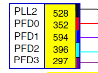
Also, in the user's manual all references to PLL-PFD3 are for 297MHz, although the register's default is the same as PFD1 (which would be 594MHz).
Looking at the clock config tool it shows 594Mz for PLL2-PFD3 (matching with the CCM_ANALOG_PFD_528 default state in the user's manual and also in the HW).
Is the user's manual at fault or is there a reason why it always reference 297MHz?
The more worrying question is whether the MAX limits as specified in the user's manual can be trusted? There are no such values in the chip's data sheet and so the only ones available are the ones in the user's manual table!!!
Regards
Mark
- Mark as New
- Bookmark
- Subscribe
- Mute
- Subscribe to RSS Feed
- Permalink
- Report Inappropriate Content
Hello,
Thanks for your information . The RM should be correct. Did you measure it with own code or the nxp example code?
Best regards
- Mark as New
- Bookmark
- Subscribe
- Mute
- Subscribe to RSS Feed
- Permalink
- Report Inappropriate Content
Hi
I tested without any code.
1. Connect debugger to the board
2. Reset the processor
3. Change CCM_CCOSR and IOMUXC_SW_MUX_CTL_PAD_GPIO_SD_B1_02 and IOMUXC_SW_PAD_CTL_PAD__GPIO_SD_B1_02 accordingly (by hand in their register views) to connect the pin to the internal source.
Regards
Mark
P.S. Note that details in the RM are contradictory - on one page it states the one default frequency and on another it shows default register selecting different defaults to those that would select this frequency.


