
- NXP Forums
- Product Forums
- General Purpose MicrocontrollersGeneral Purpose Microcontrollers
- i.MX Forumsi.MX Forums
- QorIQ Processing PlatformsQorIQ Processing Platforms
- Identification and SecurityIdentification and Security
- Power ManagementPower Management
- MCX Microcontrollers
- S32G
- S32K
- S32V
- MPC5xxx
- Other NXP Products
- Wireless Connectivity
- S12 / MagniV Microcontrollers
- Powertrain and Electrification Analog Drivers
- Sensors
- Vybrid Processors
- Digital Signal Controllers
- 8-bit Microcontrollers
- ColdFire/68K Microcontrollers and Processors
- PowerQUICC Processors
- OSBDM and TBDML
-
- Solution Forums
- Software Forums
- MCUXpresso Software and ToolsMCUXpresso Software and Tools
- CodeWarriorCodeWarrior
- MQX Software SolutionsMQX Software Solutions
- Model-Based Design Toolbox (MBDT)Model-Based Design Toolbox (MBDT)
- FreeMASTER
- eIQ Machine Learning Software
- Embedded Software and Tools Clinic
- S32 SDK
- S32 Design Studio
- Vigiles
- GUI Guider
- Zephyr Project
- Voice Technology
- Application Software Packs
- Secure Provisioning SDK (SPSDK)
- Processor Expert Software
-
- Topics
- Mobile Robotics - Drones and RoversMobile Robotics - Drones and Rovers
- NXP Training ContentNXP Training Content
- University ProgramsUniversity Programs
- Rapid IoT
- NXP Designs
- SafeAssure-Community
- OSS Security & Maintenance
- Using Our Community
-
-
- Home
- :
- i.MX Forums
- :
- i.MX Processors
- :
- DDR3 calibration issue on custom iMX6Solo board
DDR3 calibration issue on custom iMX6Solo board
- Subscribe to RSS Feed
- Mark Topic as New
- Mark Topic as Read
- Float this Topic for Current User
- Bookmark
- Subscribe
- Mute
- Printer Friendly Page
DDR3 calibration issue on custom iMX6Solo board
- Mark as New
- Bookmark
- Subscribe
- Mute
- Subscribe to RSS Feed
- Permalink
- Report Inappropriate Content
# markmiddleton
Hi Mark, The failure we're seeing mimics thread https://community.nxp.com/thread/506442 .
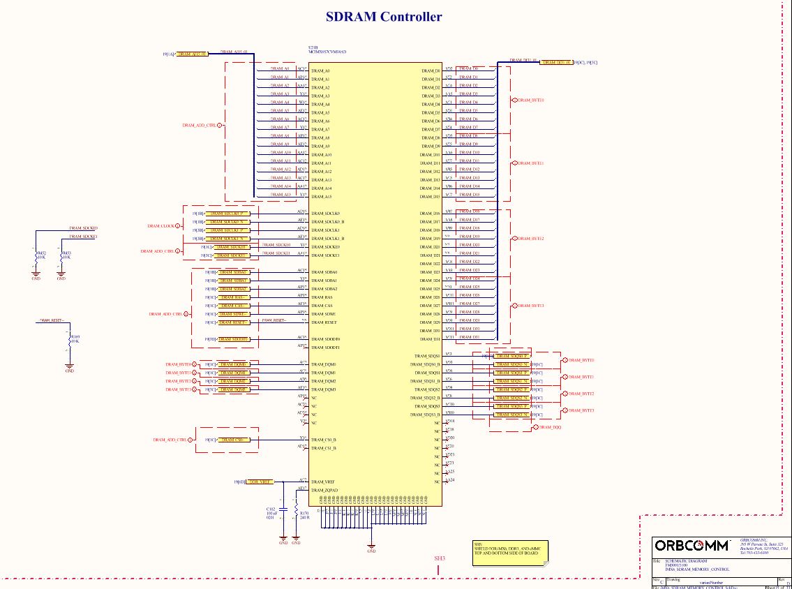
However all the required voltages are present in our case. We're using both 24 MHz and 32.768 kHz external crystals. The clocks look clean at around 1.1 Vpp. We're using two 4 Gbit DDR3 chips from Alliance operating on 1.35V. Along with the NXP iMX6 Solo processor we are using the NXP PMIC MMPF0200F6AEP. The DRAM_RESET pin is high (1.35 V). SDCKE0 and SDCKE1 are both low. DDR_VREF is 0.68 V (comes from PMIC).
Here's the test tool window:

Below is the text output of the tool after downloading the .inc script and then running the calibration:
============================================
DDR Stress Test (3.0.0)
Build: Dec 14 2018, 14:12:28
NXP Semiconductors.
============================================
============================================
Chip ID
CHIP ID = i.MX6 Solo/DualLite (0x61)
Internal Revision = TO1.4
============================================
============================================
Boot Configuration
SRC_SBMR1(0x020d8004) = 0x0100d072
SRC_SBMR2(0x020d801c) = 0x01000001
============================================
ARM Clock set to 800MHz
============================================
DDR configuration
BOOT_CFG3[5-4]: 0x00, Single DDR channel.
DDR type is DDR3
Data width: 32, bank num: 8
Row size: 15, col size: 10
Chip select CSD0 is used
Density per chip select: 1024MB
============================================
Current Temperature: 49
============================================
DDR Freq: 297 MHz
ddr_mr1=0x00000004
Start write leveling calibration...
running Write level HW calibration
MPWLHWERR register read out for factory diagnostics:
MPWLHWERR PHY0 = 0x00001e1e
HW WL cal status: no suitable delay value found for byte 2
HW WL cal status: no suitable delay value found for byte 3
Write leveling calibration completed but failed, the following results were found:
MMDC_MPWLDECTRL0 ch0 (0x021b080c) = 0x000D0013
MMDC_MPWLDECTRL1 ch0 (0x021b0810) = 0x001F001F
Write DQS delay result:
Write DQS0 delay: 19/256 CK
Write DQS1 delay: 13/256 CK
Write DQS2 delay: 31/256 CK
Write DQS3 delay: 31/256 CK
Error: failed during write leveling calibration
Since we can't get by the "simple" leveling routine, there must be something obvious that we are missing.
- Mark as New
- Bookmark
- Subscribe
- Mute
- Subscribe to RSS Feed
- Permalink
- Report Inappropriate Content
Hi Dana,
First, please do not run the DDR calibration routine much below 333 MHz.
I would recommend a setting of 350 MHz to start out with.
Please let the DDR Density setting remain at default.
Finally, set the Write DQS and Read DQS values at 0x40 for all four channels and write leveling at 0x1F and run the Stress Test a couple of times without calibration. Please report the results. Maybe there is some clue in the failing results that might help us. It looks like lanes #0 and #1 are working fine, but the other two are having problems.
Cheers,
Mark
- Mark as New
- Bookmark
- Subscribe
- Mute
- Subscribe to RSS Feed
- Permalink
- Report Inappropriate Content
Hello Mark aka The Admiral,
Thanks for the advice. After discussion with other engineers there is some confusion. First the channels you are referring to are the byte lanes, correct? Do I need to write 0x1F to each byte 0x1F1F1F1F or just 0x001F001F for the write leveling? An example of the .inc file has the following:
=============
// Calibration setup.
//=============================================================================
setmem /32 0x021b0800 = 0xA1390003 // DDR_PHY_P0_MPZQHWCTRL, enable both one-time & periodic HW ZQ calibration.
// For target board, may need to run write leveling calibration to fine tune these settings.
setmem /32 0x021b080c = 0x00000000 //my comment 0x1F1F1F1F or 0x001F001F?
setmem /32 0x021b0810 = 0x00000000 //my comment 0x1F1F1F1F or 0x001F001F?
//setmem /32 0x021b480c = 0x00000000 //my comment 0x1F1F1F1F or 0x001F001F?
//setmem /32 0x021b4810 = 0x00000000 //my comment 0x1F1F1F1F or 0x001F001F ?
////Read DQS Gating calibration
setmem /32 0x021b083c = 0x00000000 // MPDGCTRL0 PHY0 //my comment what do we write here?
setmem /32 0x021b0840 = 0x00000000 // MPDGCTRL1 PHY0 //my comment ditto?
//setmem /32 0x021b483c = 0x00000000 // MPDGCTRL0 PHY1 //my comment ditto?
//setmem /32 0x021b4840 = 0x00000000 // MPDGCTRL1 PHY1 //my comment ditto?
//Read calibration
setmem /32 0x021b0848 = 0x40404040 // MPRDDLCTL PHY0 // my comment each byte lane gets x40? This is the from the original .inc file
//setmem /32 0x021b4848 = 0x40404040 // MPRDDLCTL PHY1
//Write calibration
setmem /32 0x021b0850 = 0x40404040 // MPWRDLCTL PHY0
//setmem /32 0x021b4850 = 0x40404040 // MPWRDLCTL PHY1
Help!
Dana C. Johnson, VP PI&D
ORBCOMM, Inc. Suite 300
22970 Indian Creek Drive
Dulles, VA 20166
Office: 703-433-6456 Cell#1: 201-220-4613 Cell#2: 703-728-5939
www.orbcomm.com<http://www.orbcomm.com>; johnson.dana@orbcomm.com<mailto:johnson.dana@orbcomm.com>
- Mark as New
- Bookmark
- Subscribe
- Mute
- Subscribe to RSS Feed
- Permalink
- Report Inappropriate Content
Hi Dana,
Sorry for the confusion. Those are correct, except the Write Level calibration line should look like (0x001F001F)
Just would like to see the results with default calibration values.
Cheers,
Mark
- Mark as New
- Bookmark
- Subscribe
- Mute
- Subscribe to RSS Feed
- Permalink
- Report Inappropriate Content
- Mark as New
- Bookmark
- Subscribe
- Mute
- Subscribe to RSS Feed
- Permalink
- Report Inappropriate Content
Hi Mark,
We've been trying different things with the tool and we ran across this: change the bus width down from 32 bits to 16 bits. Include your previous recommendations. Select iMX6DL in the DDR test tool. Download our new .inc file (attached) that reflect the 16 bit bus width. Let the tool pick the ARM clock speed as well as the memory density. See below:

Run the calibration...it succeeded at 400 MHz every time but some times it fails at 350 MHz...strange! See attached log file. Ran the stress test at 400 MHz. Passed!!! See second log file.
Our memory is setup as two 4 Gbit chips organized as 256M x 16 giving us a total of 8 Gbits or 1 GByte. The first chip uses SDQS0 and SDQS1 for data strobes. The second chip uses SDQS2 and SDQS3 for the data strobes. DQM0 and DQM1 are used for the first chip and DQM2, DQM3 are used for the second chip. We noticed that a SOLOX design that uses the same memory organization as our board uses SDQS0 and SDQS2 for the first chip and SDQS1 and SDQS3 for the second chip. We didn't think that would matter but it is the only difference we have noticed.
- Mark as New
- Bookmark
- Subscribe
- Mute
- Subscribe to RSS Feed
- Permalink
- Report Inappropriate Content
Here's some additional information on our design:
1. We used one chip select CS0 for both DDR3 memory chips.
2. The low word chip uses CLK0 along with data strobes DQS0 and DQS1. It uses SDCKE0.
3. The upper word chip uses CLK1 along with data strobes DQS2 and DQS3. It uses SDCKE1.
- Mark as New
- Bookmark
- Subscribe
- Mute
- Subscribe to RSS Feed
- Permalink
- Report Inappropriate Content
Hello,
Please check Your PCB design, using section 1.1 (Schematic and Layout Design Rules)
of the DDR3 Porting Guide. In particular, there is an Excel page named “MX6 DRAM Bus Length Check”
in “HW Design Checking List for i.Mx6”. Designer can use it for layout self-checking.
Freescale i.MX6 DRAM Port Application Guide-DDR3
https://community.nxp.com/docs/DOC-93819
Have a great day,
Yuri.
-------------------------------------------------------------------------------
Note:
- If this post answers your question, please click the "Mark Correct" button. Thank you!
- We are following threads for 7 weeks after the last post, later replies are ignored
Please open a new thread and refer to the closed one, if you have a related question at a later point in time.
- Mark as New
- Bookmark
- Subscribe
- Mute
- Subscribe to RSS Feed
- Permalink
- Report Inappropriate Content
“I was surprised to see that the HW Guide design rules are NOT consistent with the HW Design Checklist Excel spreadsheet. If you put our trace lengths into the spreadsheet then there are many “failures” (cell turns RED). The checklist says <= 25 mil is the tolerance while the design guide says +/- 25 mils. I’ve attached the spreadsheet for the ORBCOMM board.
Here’s what our PCB designer said:
“I designed the trace lengths to follow the “Routing by the same length” rules from the design guide. This was the simpler method of building the rules and the fastest way to route.
If you check the values in the table, I have routed the main clocks to ~1.62”, the DSQ clocks to 1.617”, and all of the remaining signals between 1.595” and 1.645” (+/-25mils of the main clocks). This should meet the rules from that simplified rule set.
“
What guidelines should we be following?
- Mark as New
- Bookmark
- Subscribe
- Mute
- Subscribe to RSS Feed
- Permalink
- Report Inappropriate Content
