- NXP Forums
- Product Forums
- General Purpose MicrocontrollersGeneral Purpose Microcontrollers
- i.MX Forumsi.MX Forums
- QorIQ Processing PlatformsQorIQ Processing Platforms
- Identification and SecurityIdentification and Security
- Power ManagementPower Management
- MCX Microcontrollers
- S32G
- S32K
- S32V
- MPC5xxx
- Other NXP Products
- Wireless Connectivity
- S12 / MagniV Microcontrollers
- Powertrain and Electrification Analog Drivers
- Sensors
- Vybrid Processors
- Digital Signal Controllers
- 8-bit Microcontrollers
- ColdFire/68K Microcontrollers and Processors
- PowerQUICC Processors
- OSBDM and TBDML
-
- Solution Forums
- Software Forums
- MCUXpresso Software and ToolsMCUXpresso Software and Tools
- CodeWarriorCodeWarrior
- MQX Software SolutionsMQX Software Solutions
- Model-Based Design Toolbox (MBDT)Model-Based Design Toolbox (MBDT)
- FreeMASTER
- eIQ Machine Learning Software
- Embedded Software and Tools Clinic
- S32 SDK
- S32 Design Studio
- Vigiles
- GUI Guider
- Zephyr Project
- Voice Technology
- Application Software Packs
- Secure Provisioning SDK (SPSDK)
- Processor Expert Software
-
- Topics
- Mobile Robotics - Drones and RoversMobile Robotics - Drones and Rovers
- NXP Training ContentNXP Training Content
- University ProgramsUniversity Programs
- Rapid IoT
- NXP Designs
- SafeAssure-Community
- OSS Security & Maintenance
- Using Our Community
-
- Cloud Lab Forums
-
- Home
- :
- Power Management
- :
- Power Management
- :
- Spikes on switch 3 during ramp-up - using KITPF8100FRDMEVM
Spikes on switch 3 during ramp-up - using KITPF8100FRDMEVM
- Subscribe to RSS Feed
- Mark Topic as New
- Mark Topic as Read
- Float this Topic for Current User
- Bookmark
- Subscribe
- Mute
- Printer Friendly Page
Spikes on switch 3 during ramp-up - using KITPF8100FRDMEVM
- Mark as New
- Bookmark
- Subscribe
- Mute
- Subscribe to RSS Feed
- Permalink
- Report Inappropriate Content
Customer: SICK (Germany)
Platform: i.MX 8M-Mini + PF8200 (for safety purposes)
I got a question from SICK with regards to the PF8200. They work on the PF8100 FRDM EVM and have seen the following behavior:
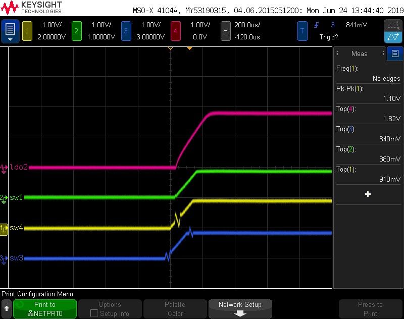
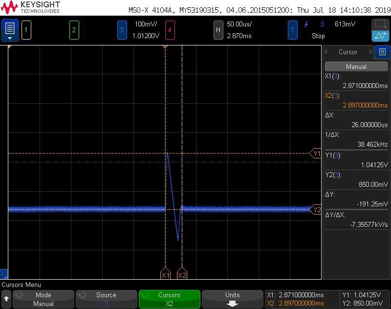
During the power up sequence, some switches have voltage spikes during ramp ups. But the buck converter switch 3 (blue curve) has a spike at the regulated voltage as seen from the picture below:
Now this voltage from buck 3 goes to the i.MX 8M-Mini and it would be helpful to know why this happens. This spike does not happen when only switch 3 is ON and rest of the bucks are off.
- Mark as New
- Bookmark
- Subscribe
- Mute
- Subscribe to RSS Feed
- Permalink
- Report Inappropriate Content
HI
I suggest your test in only EVB of KITPF8100FRDMEVM with or without load to verify this overshoot in startup stage of SW3.
Perhaps long wire connection between PMIC and I.MX will bring this.
Thanks!
- Mark as New
- Bookmark
- Subscribe
- Mute
- Subscribe to RSS Feed
- Permalink
- Report Inappropriate Content
Hi G.W.
customer did some further tests on the PF8200 eval kit, see below.
The problem they have is finally related to their own hardware implementation. They do a design for the i.MX8M-Mini + PF8200, in about two weeks from now they will get their hardware and want to validate it.
But the spikes reach a voltage level which is outside the spec for 8M-Mini power supply inputs.
It could be related to a measurement problem, the design of the KITPF8100FRDMEVM or the PF8200 itself.
The concern from SICK is, that this effect also exists on their board and that they could damage something when they put it into operation..
Customer report:
Measurements were done like shown in the graphic.
The first picture is when Switches 3, 4, 1 and LDO2 are measured (other LDOs are off, switches 2,5,6,7 are on). Here you see that there is a spike in switch 3 when switch 4 turns on and there is a spike in switch 4 when LDO2 turns on. It occurs only with buck 3 and 4 and not with any other bucks.
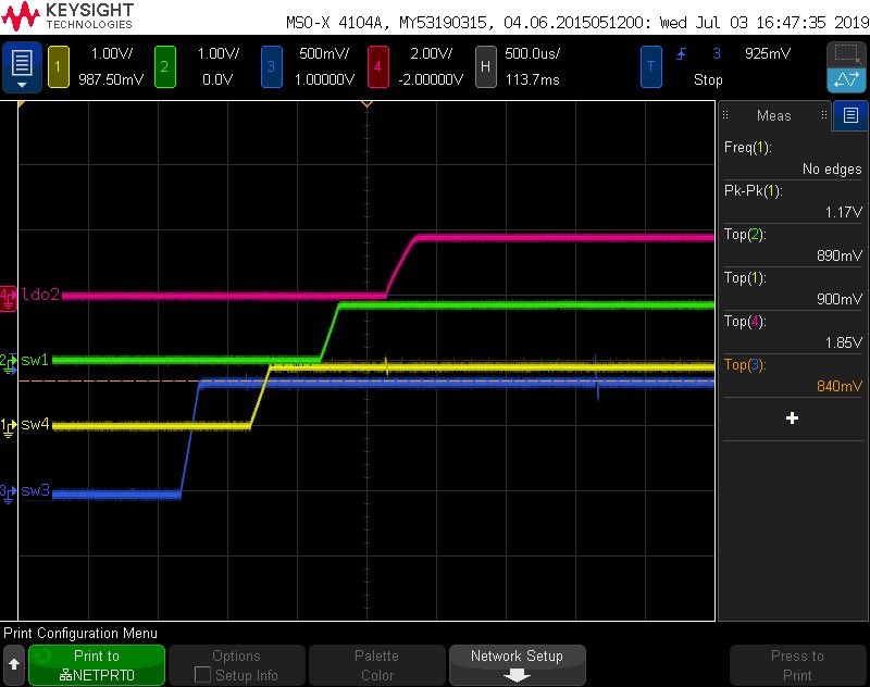
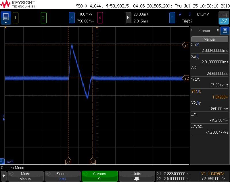
Here you see a spike on switch 3 when switch 2 turns ON. I have used the standard oscilloscope probes here and measured without load. I'm using GND pads close to the signal measurement points to avoid parasitic effects:
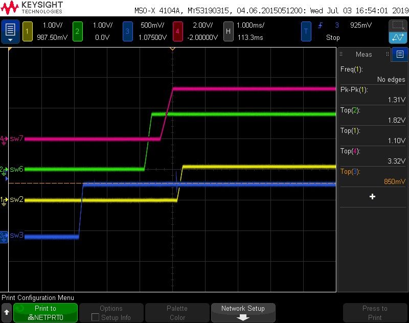
As per your advice in your previous email, I used very short loops between the signal measurement points and the ground points using the MSO4104 scope and tested it without any load. I measured just the switch 3 which had the biggest spike. (Other switches were on as well).
A screenshot of it is below. This spike appears when switch 2 is turned on.
I powered the board from an external power supply port and from the USB port. The spike is there in both cases.
The switches which have the spike are just 3 and 4, the rest of the switches are not affected.
- In total there are 3 spikes that happen:
SW3 spikes when SW4 turns on
SW3 spikes when SW2 turns on
SW4 spikes when LDO2 turns on.
Regards,
Bernhard.
- Mark as New
- Bookmark
- Subscribe
- Mute
- Subscribe to RSS Feed
- Permalink
- Report Inappropriate Content
Hi,
About the spike issue on SW3 regulator you are seen during the ramp up…
Bernard did a very good point mentioning that customer should use a good probe and use a GND connection as close as possible to the signal measurement point and use a short connection.
I believe that customer is seen this ripple because of the way it’s being measured, please correct me if I’m wrong, but I think that customer is measuring using an oscilloscope probe connecting the GND connection to one random point of ground in the board and the end of the probe on one point of the SW3 output of the board, right?
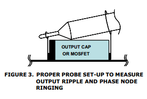
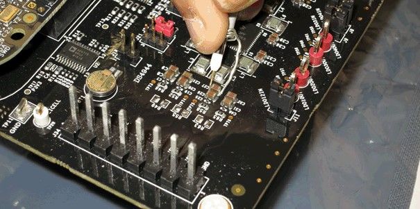
Now, remember that Buck regulators as SW3 are high speed switching signals, so care must be taken when measuring this kind of signals, just by measuring using a close GND reference on the board could not be enough to eliminate the ripple out of the measuring, you would need to reduce the space of the measurement between the GND and the end of the probe by placing a cable around the probe ground closer to the end as mentioned in the following image:
Please confirm when customer make the measurements using this method and send me the updated waveforms.
If the problem persist, I’ll check other possible causes with the Applications team.
Thanks,
Jose Alberto Reyes
Technical Information Center
Analog and Sensors Support Engineer
- Mark as New
- Bookmark
- Subscribe
- Mute
- Subscribe to RSS Feed
- Permalink
- Report Inappropriate Content
Hi Jose,
Customer confirmed that they measured close to the power source.
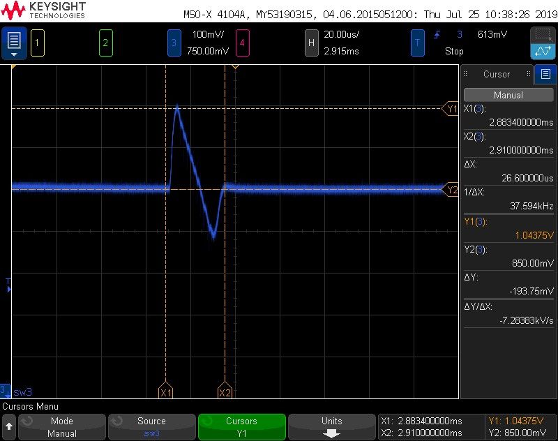
I did the measurements again as you suggested in the graphic yesterday and I am attaching two results here. One measured wit thr oscilloscope probe connected normally by using a close GND reference on board and the second one using a short measurement path between signal and ground.
1. Normal measurement using a nearby GND reference on board
2. Switch 3 signal measured across the capacitor using a small measurement path. The spike on this switch 3 still exists (switch 2 turning on at that point)
Regards,
Bernhard.
- Mark as New
- Bookmark
- Subscribe
- Mute
- Subscribe to RSS Feed
- Permalink
- Report Inappropriate Content
Hi Bernhard,
This is the response I received from the Apps team:
This is a known behavior that we found recently,
See attached Power point , it describe the behavior on the production silicon (official errata is being put together as we speak).
however, on B0 silicon , the behavior is present on different combinations of regulator being enabled.
summarizing the behavior:
this is related to the routing of the bias signals of the SW regulators, LDOS, and their OV/UV monitors. so when these signals are running parallel to each other without any shielding, the glitch will be present when the regulator is enabled, or the OV/UV mon is enabled (which typically happen together when the Regulator is enabled, but the OV/UV monitors can be disabled and enabled independently if needed)
in your plot, what is happening is that the regulator are creating this cross talk when the other regulators are being enabled in the sequence.
on C0/C1 production silicon, we work to fix this issue, unfortunately there is one condition we did not spot during the fix and hence the errata on C0 silicon.
- Mark as New
- Bookmark
- Subscribe
- Mute
- Subscribe to RSS Feed
- Permalink
- Report Inappropriate Content
Hi Bernhard,
There are no reports of similar failures using the PF8200, I’ll contact the Applications engineers to see if they can help with more suggestions about possible causes of the problem.
I’ll contact you back when I receive an answer from them.
Regards,
Jose
