- NXP Forums
- Product Forums
- General Purpose MicrocontrollersGeneral Purpose Microcontrollers
- i.MX Forumsi.MX Forums
- QorIQ Processing PlatformsQorIQ Processing Platforms
- Identification and SecurityIdentification and Security
- Power ManagementPower Management
- MCX Microcontrollers
- S32G
- S32K
- S32V
- MPC5xxx
- Other NXP Products
- Wireless Connectivity
- S12 / MagniV Microcontrollers
- Powertrain and Electrification Analog Drivers
- Sensors
- Vybrid Processors
- Digital Signal Controllers
- 8-bit Microcontrollers
- ColdFire/68K Microcontrollers and Processors
- PowerQUICC Processors
- OSBDM and TBDML
-
- Solution Forums
- Software Forums
- MCUXpresso Software and ToolsMCUXpresso Software and Tools
- CodeWarriorCodeWarrior
- MQX Software SolutionsMQX Software Solutions
- Model-Based Design Toolbox (MBDT)Model-Based Design Toolbox (MBDT)
- FreeMASTER
- eIQ Machine Learning Software
- Embedded Software and Tools Clinic
- S32 SDK
- S32 Design Studio
- Vigiles
- GUI Guider
- Zephyr Project
- Voice Technology
- Application Software Packs
- Secure Provisioning SDK (SPSDK)
- Processor Expert Software
-
- Topics
- Mobile Robotics - Drones and RoversMobile Robotics - Drones and Rovers
- NXP Training ContentNXP Training Content
- University ProgramsUniversity Programs
- Rapid IoT
- NXP Designs
- SafeAssure-Community
- OSS Security & Maintenance
- Using Our Community
-
-
- Home
- :
- Product Forums
- :
- Digital Signal Controllers
- :
- SRAM for MC56F8367
SRAM for MC56F8367
- Subscribe to RSS Feed
- Mark Topic as New
- Mark Topic as Read
- Float this Topic for Current User
- Bookmark
- Subscribe
- Mute
- Printer Friendly Page
SRAM for MC56F8367
- Mark as New
- Bookmark
- Subscribe
- Mute
- Subscribe to RSS Feed
- Permalink
- Report Inappropriate Content
Hi
I am using two 128K X 16 Asynchronous SRAM for my project with mc56f8367 (codewarrior 10.7).
I am unable to find any example code to store and access data from sram.
I am facing trouble while programming. Can anyone help me .
Thanks in advance.
- Mark as New
- Bookmark
- Subscribe
- Mute
- Subscribe to RSS Feed
- Permalink
- Report Inappropriate Content
Hi Padma
It would be helpful to know how you have the SRAM chips connected to the DSC.
As Xiangjun Rong pointed out above, what CS lines are you using to access the SRAM.
A schematic or description would be good.
The example Code in CS_56F8367_PE.c (IN the attached file above) is very straightforward pointer access to memory:
These 2 lines define the location in memory (the second one could be SRAM).
unsigned int * IOPointer=(unsigned int *)0x0008010;
unsigned int * RAMPointer=(unsigned int *)0x0D10000;
These 2 lines write values to the locations.
(*IOPointer)=0x1234; //base address is 008 Hex in cpu bean
(*RAMPointer)=0x5678; //base address is D10 Hex
If you want to read from the locations you define a variable and then assign the value at the memory location to the variable.
Create the var.
unsigned int MemValue;
Assign a memory location value to the var.
MemValue = *RAMPointer;
So if RAMPointer had 0x5678 in it, now MemValue would have 0x5678 in it.
Hope this help some.
Pete
- Mark as New
- Bookmark
- Subscribe
- Mute
- Subscribe to RSS Feed
- Permalink
- Report Inappropriate Content
Hi, Padma,
For detailed information about the Asynchronous SRAM, pls refer to the Chapter 4
External Memory Interface (EMI).
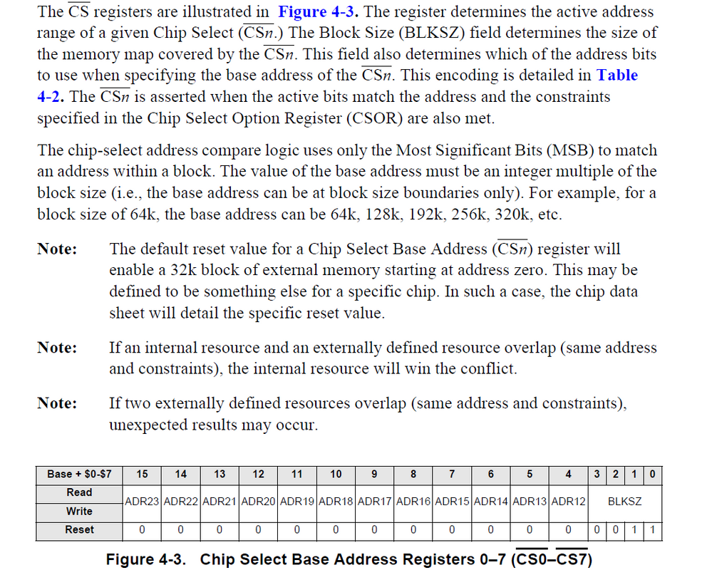
Pls refer to the figure 4-3, you use 128K*16 bits SRAM, the memory address is from A0~A16, the A17~A23 are used to decode the /CS signal. I suppose for example, you use /CS2 for one 128K SRAM, /CS3 for another 128K SRAM.
1)For /CS1, you can use the address:
A23 A22 A21 A20 A19 A18 A17 A16.................
0 0 0 1 1 1 1
You can access the 0x00 0000 to 0x 1E 0000 as the /CS2 address
You can set the Chip Select Base Address Registers 2 as 0x1E05
For /CS2, you can use the address:
A23 A22 A21 A20 A19 A18 A17 A16.................
0 0 0 1 1 1 0
You can access the 0x00 0000 to 0x1C 0000 as the /CS3 address
You can set the Chip Select Base Address Registers 2 as 0x1C05
For the other register, you can set based on your requirement.
You can PE to set the EMI register.
Hope it can help you
BR
XiangJun Rong
- Mark as New
- Bookmark
- Subscribe
- Mute
- Subscribe to RSS Feed
- Permalink
- Report Inappropriate Content
Hi
Thankyou. Still i find difficulties while programming as i have not used sram before.
Kindly can you send me a simple program to write a data and read that same data from sram.
- Mark as New
- Bookmark
- Subscribe
- Mute
- Subscribe to RSS Feed
- Permalink
- Report Inappropriate Content
- Mark as New
- Bookmark
- Subscribe
- Mute
- Subscribe to RSS Feed
- Permalink
- Report Inappropriate Content
Hi,
There is no example code for mc56f8367 SRAM module in codewarrior 11.1 package.
