- NXP Forums
- Product Forums
- General Purpose MicrocontrollersGeneral Purpose Microcontrollers
- i.MX Forumsi.MX Forums
- QorIQ Processing PlatformsQorIQ Processing Platforms
- Identification and SecurityIdentification and Security
- Power ManagementPower Management
- MCX Microcontrollers
- S32G
- S32K
- S32V
- MPC5xxx
- Other NXP Products
- Wireless Connectivity
- S12 / MagniV Microcontrollers
- Powertrain and Electrification Analog Drivers
- Sensors
- Vybrid Processors
- Digital Signal Controllers
- 8-bit Microcontrollers
- ColdFire/68K Microcontrollers and Processors
- PowerQUICC Processors
- OSBDM and TBDML
-
- Solution Forums
- Software Forums
- MCUXpresso Software and ToolsMCUXpresso Software and Tools
- CodeWarriorCodeWarrior
- MQX Software SolutionsMQX Software Solutions
- Model-Based Design Toolbox (MBDT)Model-Based Design Toolbox (MBDT)
- FreeMASTER
- eIQ Machine Learning Software
- Embedded Software and Tools Clinic
- S32 SDK
- S32 Design Studio
- Vigiles
- GUI Guider
- Zephyr Project
- Voice Technology
- Application Software Packs
- Secure Provisioning SDK (SPSDK)
- Processor Expert Software
-
- Topics
- Mobile Robotics - Drones and RoversMobile Robotics - Drones and Rovers
- NXP Training ContentNXP Training Content
- University ProgramsUniversity Programs
- Rapid IoT
- NXP Designs
- SafeAssure-Community
- OSS Security & Maintenance
- Using Our Community
-
-
- Home
- :
- General Purpose Microcontrollers
- :
- Kinetis Microcontrollers
- :
- Apparent conflict in DMA documentation K22P144M120SF5V2RM
Apparent conflict in DMA documentation K22P144M120SF5V2RM
- Subscribe to RSS Feed
- Mark Topic as New
- Mark Topic as Read
- Float this Topic for Current User
- Bookmark
- Subscribe
- Mute
- Printer Friendly Page
Apparent conflict in DMA documentation K22P144M120SF5V2RM
- Mark as New
- Bookmark
- Subscribe
- Mute
- Subscribe to RSS Feed
- Permalink
- Report Inappropriate Content
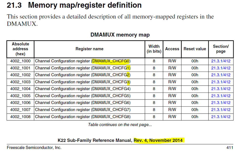
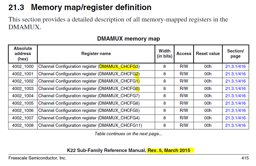
In the document, K22P144M120SF5V2RM.pdf, Rev 5 2015, in section 21.3 Memory map is listed DMA MUX channel configuration registers this shows 0x4002_1000 to channel 3, 0x4002_1001 to channel 2, etc.
An example on page 422 shows the expected mapping of 0x4002_1000 to channel 0, 0x4002_1001 to channel 1, etc.
Example eDMA code shows 0x4002_1000 map to channel 0.
Which mapping is correct?
- Mark as New
- Bookmark
- Subscribe
- Mute
- Subscribe to RSS Feed
- Permalink
- Report Inappropriate Content
Hi Keith
That is interesting:
However, in the change notes:
I have always used the Rev.4 addressing for K22F product development and never had an issue, but maybe there are differences between chips since the Rev.4 is for devices called (for example) MK22FX512VLQ12 and the Rev.5 for devices called (for example) MK22FX512AVLQ12.
To be sure, try with the Rev.4 set and in case of difficulties have a go at changing the order (which I never needed to try).
Regards
Mark
uTasker developer and supporter (+5'000 hours experience on +60 Kinetis derivatives in +80 product developments)
Kinetis: http://www.utasker.com/kinetis.html
- Mark as New
- Bookmark
- Subscribe
- Mute
- Subscribe to RSS Feed
- Permalink
- Report Inappropriate Content
In looking back at the document, the access order is correct with 'big endian' and 32-bit, I believe. However, the entire document uses character pointers, so it is confusing. There are other tables with the same 0-1-2-3 mapping to 3-2-1-0.
- Mark as New
- Bookmark
- Subscribe
- Mute
- Subscribe to RSS Feed
- Permalink
- Report Inappropriate Content
Hi Keith Smith,
Got confirmation from design, the memory map table in Rev 5 content is wrong, and the example code and memory map table in Rev 4 are correct. This issue was recorded in system, will update the RM when getting enough issues or 3 months later without further issue reported. Thanks!
Best Regards,
Robin
- Mark as New
- Bookmark
- Subscribe
- Mute
- Subscribe to RSS Feed
- Permalink
- Report Inappropriate Content
Robin,
As long as we are looking at documentation, can you check out the actual operation of the DAC interval timer in the PDB module? I had also noticed the discrepancy. Re: https://community.nxp.com/message/413598?q=pdb%20dac
Also, I spent several hours trying to get the DMA to write to the bitband region of GPIO. I ended up searching the community board to find out that the ref manual says it wasn't possible. It took me a while to find that in the ref manual. It all came down to misunderstanding the difference between bitband region and aliased bitband region as shown in Table 4-1. Maybe the table should show, for example, 0x4000_0000-0x4007_FFFF AIPS0 ( can also be accessed via aliased bitband).
Mike
- Mark as New
- Bookmark
- Subscribe
- Mute
- Subscribe to RSS Feed
- Permalink
- Report Inappropriate Content
Sorry for the inconvenience!
I've contacted with the internal team for confirming. And I will inform you as soon as I get any feedback.
Best Regards,
Robin
- Mark as New
- Bookmark
- Subscribe
- Mute
- Subscribe to RSS Feed
- Permalink
- Report Inappropriate Content
Robin,
You might also ask them about the size of the DAC buffer. The rev 5 doc says only two, but I see the standard 16.
Mike


