- NXP Forums
- Product Forums
- General Purpose MicrocontrollersGeneral Purpose Microcontrollers
- i.MX Forumsi.MX Forums
- QorIQ Processing PlatformsQorIQ Processing Platforms
- Identification and SecurityIdentification and Security
- Power ManagementPower Management
- MCX Microcontrollers
- S32G
- S32K
- S32V
- MPC5xxx
- Other NXP Products
- Wireless Connectivity
- S12 / MagniV Microcontrollers
- Powertrain and Electrification Analog Drivers
- Sensors
- Vybrid Processors
- Digital Signal Controllers
- 8-bit Microcontrollers
- ColdFire/68K Microcontrollers and Processors
- PowerQUICC Processors
- OSBDM and TBDML
-
- Solution Forums
- Software Forums
- MCUXpresso Software and ToolsMCUXpresso Software and Tools
- CodeWarriorCodeWarrior
- MQX Software SolutionsMQX Software Solutions
- Model-Based Design Toolbox (MBDT)Model-Based Design Toolbox (MBDT)
- FreeMASTER
- eIQ Machine Learning Software
- Embedded Software and Tools Clinic
- S32 SDK
- S32 Design Studio
- Vigiles
- GUI Guider
- Zephyr Project
- Voice Technology
- Application Software Packs
- Secure Provisioning SDK (SPSDK)
- Processor Expert Software
-
- Topics
- Mobile Robotics - Drones and RoversMobile Robotics - Drones and Rovers
- NXP Training ContentNXP Training Content
- University ProgramsUniversity Programs
- Rapid IoT
- NXP Designs
- SafeAssure-Community
- OSS Security & Maintenance
- Using Our Community
-
-
- Home
- :
- MCUXpresso Software and Tools
- :
- MCUXpresso IDE
- :
- Can not flash LPC1833 with LPC-link 2
Can not flash LPC1833 with LPC-link 2
- Subscribe to RSS Feed
- Mark Topic as New
- Mark Topic as Read
- Float this Topic for Current User
- Bookmark
- Subscribe
- Mute
- Printer Friendly Page
Can not flash LPC1833 with LPC-link 2
- Mark as New
- Bookmark
- Subscribe
- Mute
- Subscribe to RSS Feed
- Permalink
- Report Inappropriate Content
Hi,
I am using MCUXpresso IDE v10.1.0 [Build 589] [2017-11-14]
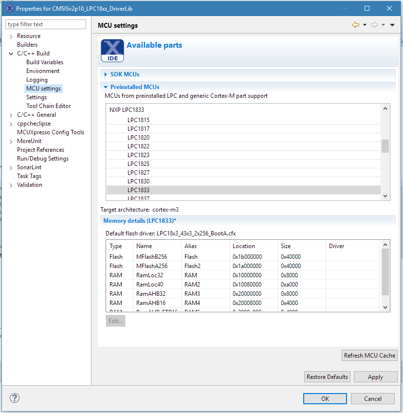
I am trying to flash LPC 1833 with below memory configuration
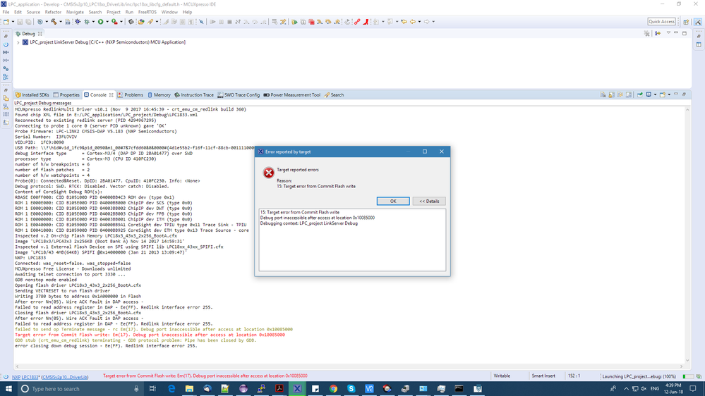
Now when I am trying to flash image using "LINK server GUI Flash Programmer", I am getting errors as below
My LPC link-2 is configured as CMSIS-DAP.
Also, Note that when I try to erase Partition A or Partition B am getting Successful operation. Problem occurs when i try to write one of the Partition.
Please help me on this!
Thanks,
Shalin
- Mark as New
- Bookmark
- Subscribe
- Mute
- Subscribe to RSS Feed
- Permalink
- Report Inappropriate Content
Please boot your board into ISP mode. Then immediately - without using FlashMagic - try to start a debug session.
Regards,
MCUXpresso IDE Support
- Mark as New
- Bookmark
- Subscribe
- Mute
- Subscribe to RSS Feed
- Permalink
- Report Inappropriate Content
Hi,
Thanks for the help!
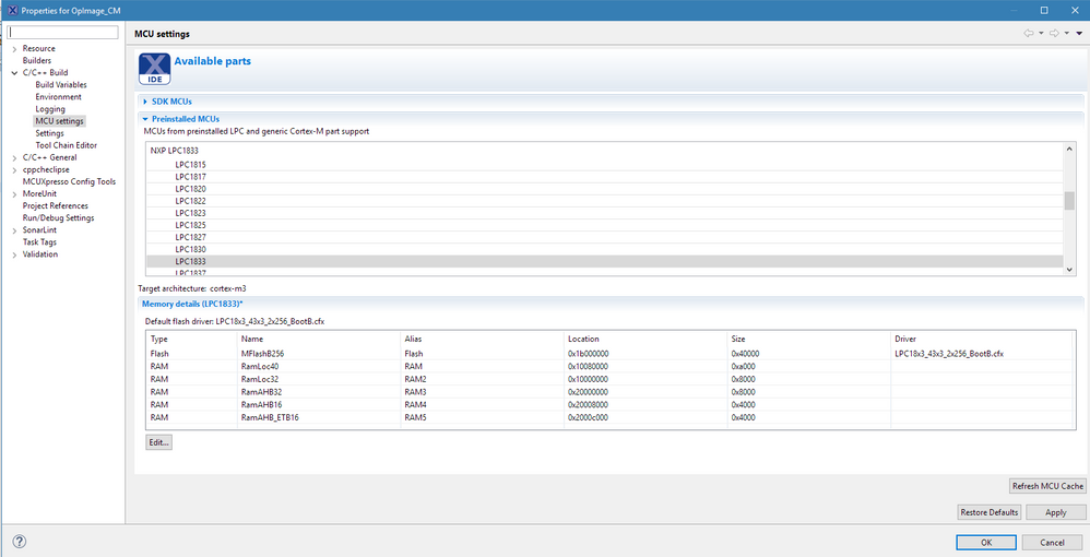
But still even after setting Memory region to just one flash location from where my application is going to execute as below,
i am getting error when I am trying to flash image in partition B using "LINK server GUI Flash Programmer" as below
//****************************************************************************************************************************//
Ns: MCUXpresso RedlinkMulti Driver v10.1 (Nov 9 2017 16:45:39 - crt_emu_cm_redlink.exe build 360)
Pc: ( 0) Reading remote configuration
Wc(03). No cache support.
Nc: Found chip XML file in E:/Cosmos/CM_1.50.0.0.0.0/source/cm_op_image/OpImage_CM/Release\LPC1833.xml
Pc: ( 5) Remote configuration complete
Nc: Reconnected to existing redlink server (PID 4294967295)
Nc: Connecting to probe 1 core 0 (server PID unknown) gave 'OK'
Nc: Probe Firmware: LPC-LINK2 CMSIS-DAP V5.183 (NXP Semiconductors)
Nc: Serial Number: I3FUJVIV
Nc: VID:PID: 1FC9:0090
Nc: USB Path: \\?\hid#vid_1fc9&pid_0090&mi_00#7&7cfdd60&0&0000#{4d1e55b2-f16f-11cf-88cb-001111000030}
Pc: ( 30) Emulator Connected
Pc: ( 40) Debug Halt
Pc: ( 50) CPU ID
Nc: debug interface type = Cortex-M3/4 (DAP DP ID 2BA01477) over SWD
Nc: processor type = Cortex-M3 (CPU ID 410FC230)
Nc: number of h/w breakpoints = 6
Nc: number of flash patches = 2
Nc: number of h/w watchpoints = 4
Nc: Probe(0): Connected&Reset. DpID: 2BA01477. CpuID: 410FC230. Info: <None>
Nc: Debug protocol: SWD. RTCK: Disabled. Vector catch: Disabled.
Ns: Content of CoreSight Debug ROM(s):
Nc: RBASE E00FF000: CID B105100D PID 04000BB4C3 ROM dev (type 0x1)
Nc: ROM 1 E000E000: CID B105E00D PID 04000BB000 ChipIP dev SCS (type 0x0)
Nc: ROM 1 E0001000: CID B105E00D PID 04003BB002 ChipIP dev DWT (type 0x0)
Nc: ROM 1 E0002000: CID B105E00D PID 04002BB003 ChipIP dev FPB (type 0x0)
Nc: ROM 1 E0000000: CID B105E00D PID 04003BB001 ChipIP dev ITM (type 0x0)
Nc: ROM 1 E0040000: CID B105900D PID 04000BB9A1 CoreSight dev TPIU type 0x11 Trace Sink - TPIU
Nc: ROM 1 E0041000: CID B105900D PID 04000BB925 CoreSight dev ETM type 0x13 Trace Source - core
Nc: Inspected v.2 On-chip Flash Memory LPC18x3_43x3_2x256_BootB.cfx
Nc: Image 'LPC18x3/LPC43x3 2x256KB (Boot Bank B) Nov 14 2017 14:59:33'
Nc: NXP: LPC1833
Pc: ( 65) Chip Setup Complete
Nt: Connected: was_reset=false. was_stopped=true
Cr:v MCUXpresso Free License - Downloads unlimited
Pc: ( 70) License Check Complete
Nt: Loading 'OpImage_CM.bin' Binary 0x1B000000 len 0x21754
Nc: Opening flash driver LPC18x3_43x3_2x256_BootB.cfx
Nc: Sending VECTRESET to run flash driver
Nt: Writing 137044 bytes to address 0x1B000000 in Flash
Pb: ( 0) Mass erasing Flash
Nt: Mass erased flash in 213msec
Pb: 1 of 1 ( 0) Writing pages 11-20 at 0x1B000000 with 137044 bytes
Ps: ( 0) at 1B000000: 0 bytes - 0/137044
Nc: After error Nn(05). Wire ACK Fault in DAP access -
Nc: Failed to read address register in DAP - Ee(FF). Redlink interface error 255.
Nc: Closing flash driver LPC18x3_43x3_2x256_BootB.cfx
Nc: After error Nn(05). Wire ACK Fault in DAP access -
Nc: Failed to read address register in DAP - Ee(FF). Redlink interface error 255.
Wc: failed to send op Terminate message - rc Em(17). Debug port inaccessible after access at location 0x10085000
Pb: (100) Writing Flash ended with an error.
Ed:05: File 'OpImage_CM.bin' load failure: Em(17). Debug port inaccessible after access at location 0x10085000
Pc: (100) Target Connection Failed
Nc: error closing down debug session - Ee(FF). Redlink interface error 255.
//****************************************************************************************************************************//
still not getting why i am receiving this errors while writing to Partition B, while Erase operation is working fine!
Regards,
Shalin
- Mark as New
- Bookmark
- Subscribe
- Mute
- Subscribe to RSS Feed
- Permalink
- Report Inappropriate Content
Have you tried doing an ISP boot of your board, before starting your debug session?
If you can't make ISP boot work, then can you:
- Use the new project wizard to create a new LPC1833 project
- Build that project.
- Now use the GUI Flash Programmer (with IDE v10.1) or GUI Flash Tool (with IDE v10.2) and see if you can do a full mass erase of the device.
- Having mass erased the device, power the board down and back up again. And now see if you can program your actual application successfully
Regards,
MCUXpresso IDE Support
- Mark as New
- Bookmark
- Subscribe
- Mute
- Subscribe to RSS Feed
- Permalink
- Report Inappropriate Content
One correction to above reply i was updating ".bin" binary image not ".axf" file in "LINK server GUI Flash Programmer".
- Mark as New
- Bookmark
- Subscribe
- Mute
- Subscribe to RSS Feed
- Permalink
- Report Inappropriate Content
Yes, I have tried booting my board in ISP mode and then i have flashed it using flash magic tool. it works fine.
And also followed the steps mentioned above,
- created new project with LPC1833 MCU selected with CMSIS_LPC18xx_DriverLib
- created new launch configuration using MCUXpresso IDE Linkserver (inc. CMSIS-DAP) probes
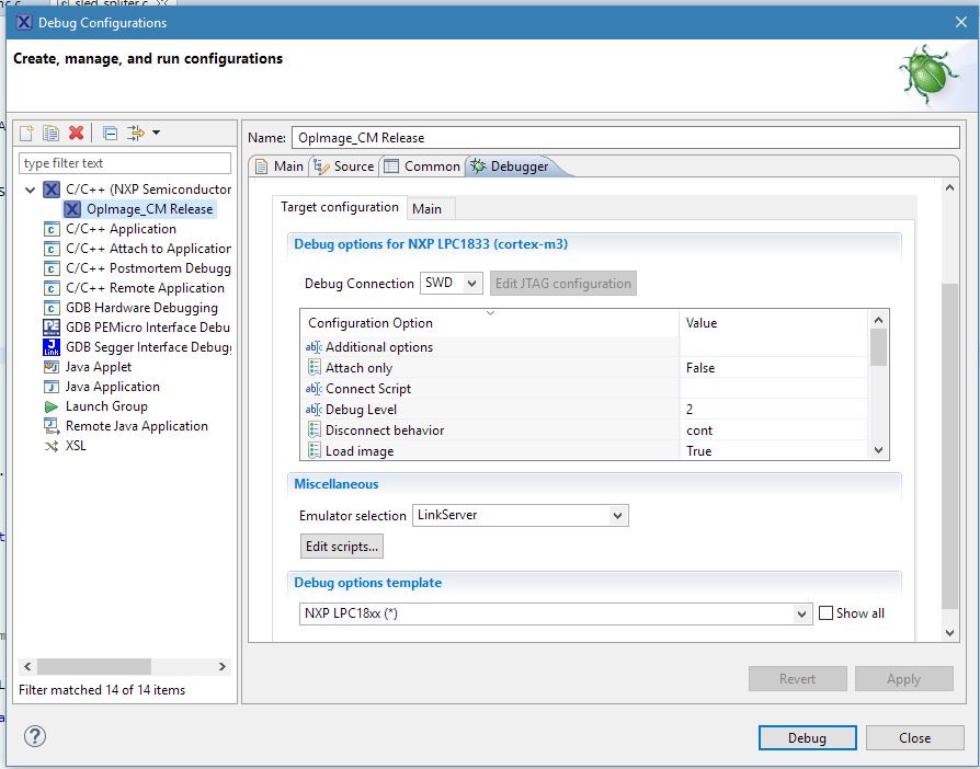
- and Debug configuration tool setting as below,
- still after mass erase using "LINK server GUI Flash Programmer" and followed power cycle MCU, I am not able to flash partition A or Partition B using "LINK server GUI Flash Programmer".
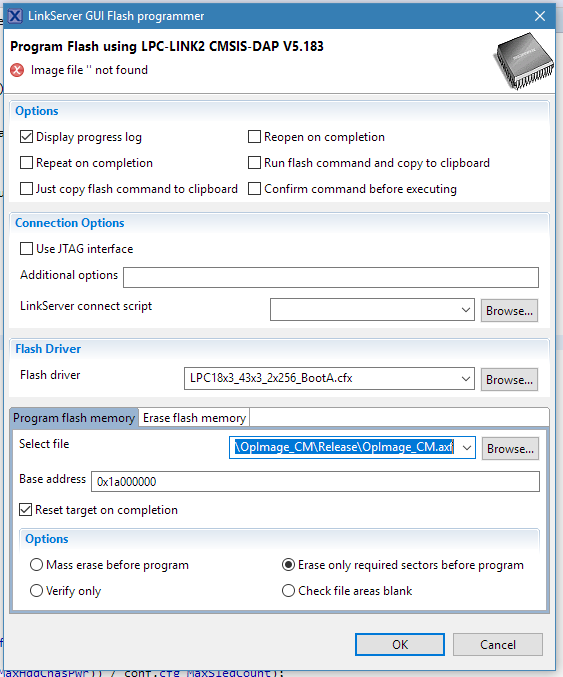
As shown in below image, Are there any requirement for Linkserver connect script (.scp) file for LPC-link2? Or any other setting is required?
Thanks,
shalin.
- Mark as New
- Bookmark
- Subscribe
- Mute
- Subscribe to RSS Feed
- Permalink
- Report Inappropriate Content
From the screenshots you have posted, its possible that the problem is being triggered by the fact that you are using both a "default" flash driver (for internal flash) and a memory region specific driver (for SPIFI). You should not mix these - as described in section 14.1, "Default vs Per-region Flash Drivers".
Try deleting the default driver in the Memory Configuration editor, and add the same flash driver to the "Flash" and "Flash2" regions.
The fact that you have reordered the two internal flash banks, but are then trying to use the "bootA" flash driver also does not look right to me - as your application will be placing code into bankB with this memory ordering. See the MCUXpresso IDE v10.2 User Guide, section 14.2.1, "LPC18xx/LPC43xx Internal Flash Drivers" for more details of these drivers.
Finally, I would suggest booting your MCU into ISP mode before making another debug connection (seeRegaining debug access to target MCU ) and also checking you have no copies of the debug executables still running in the background after the error you got (see MCUXpresso IDE v10.2 User Guide, section 18.10, "Using and troubleshooting LPC-Link2" for more info).
Regards,
MCUXpresso IDE Support
