- NXP Forums
- Product Forums
- General Purpose MicrocontrollersGeneral Purpose Microcontrollers
- i.MX Forumsi.MX Forums
- QorIQ Processing PlatformsQorIQ Processing Platforms
- Identification and SecurityIdentification and Security
- Power ManagementPower Management
- MCX Microcontrollers
- S32G
- S32K
- S32V
- MPC5xxx
- Other NXP Products
- Wireless Connectivity
- S12 / MagniV Microcontrollers
- Powertrain and Electrification Analog Drivers
- Sensors
- Vybrid Processors
- Digital Signal Controllers
- 8-bit Microcontrollers
- ColdFire/68K Microcontrollers and Processors
- PowerQUICC Processors
- OSBDM and TBDML
-
- Solution Forums
- Software Forums
- MCUXpresso Software and ToolsMCUXpresso Software and Tools
- CodeWarriorCodeWarrior
- MQX Software SolutionsMQX Software Solutions
- Model-Based Design Toolbox (MBDT)Model-Based Design Toolbox (MBDT)
- FreeMASTER
- eIQ Machine Learning Software
- Embedded Software and Tools Clinic
- S32 SDK
- S32 Design Studio
- Vigiles
- GUI Guider
- Zephyr Project
- Voice Technology
- Application Software Packs
- Secure Provisioning SDK (SPSDK)
- Processor Expert Software
-
- Topics
- Mobile Robotics - Drones and RoversMobile Robotics - Drones and Rovers
- NXP Training ContentNXP Training Content
- University ProgramsUniversity Programs
- Rapid IoT
- NXP Designs
- SafeAssure-Community
- OSS Security & Maintenance
- Using Our Community
-
-
- Home
- :
- General Purpose Microcontrollers
- :
- LPC Microcontrollers
- :
- GPIO Protection - High Voltage Input Circuit
GPIO Protection - High Voltage Input Circuit
- Subscribe to RSS Feed
- Mark Topic as New
- Mark Topic as Read
- Float this Topic for Current User
- Bookmark
- Subscribe
- Mute
- Printer Friendly Page
GPIO Protection - High Voltage Input Circuit
- Mark as New
- Bookmark
- Subscribe
- Mute
- Subscribe to RSS Feed
- Permalink
- Report Inappropriate Content
Hello all,
(Device: LPC1778fet180)
we want to connect a data line with a high voltage level (above 5 V) to P1[1]. To keep the circuit as simple (and cheap) as possible we have the idea to use a serial resistor - to limit the current - and the protection circuit on the chip - which limits the voltage.
- Is it allowed to drive the input with a current source and let the protection circuit "adjust" the voltage?
- If yes: Wich current is allowed?
- I fond in the datasheet the value I_latch (I/O latch-up current). What is the special meaning of it (What current under which condition)?
Thanks in advance,
Andreas
- Mark as New
- Bookmark
- Subscribe
- Mute
- Subscribe to RSS Feed
- Permalink
- Report Inappropriate Content
This is my original question
https://community.nxp.com/message/750299?commentID=750299#comment-750299
which is much the same as you're asking now, and I'm still none-the-wiser having received the reply from NXP.
- Mark as New
- Bookmark
- Subscribe
- Mute
- Subscribe to RSS Feed
- Permalink
- Report Inappropriate Content
Hi Ian,
I am still checking with LPC product team about this issue.
I will updated this thread when I could get any feedback.
best regards,
Mike
- Mark as New
- Bookmark
- Subscribe
- Mute
- Subscribe to RSS Feed
- Permalink
- Report Inappropriate Content
Hi all,
Sorry for the later reply.
Unfortunately, LPC product team doesn't have ESD diode allowed current data.
Have a great day,
Mike
-----------------------------------------------------------------------------------------------------------------------
Note: If this post answers your question, please click the Correct Answer button. Thank you!
-----------------------------------------------------------------------------------------------------------------------
- Mark as New
- Bookmark
- Subscribe
- Mute
- Subscribe to RSS Feed
- Permalink
- Report Inappropriate Content
Really? Can't you afford a zener?
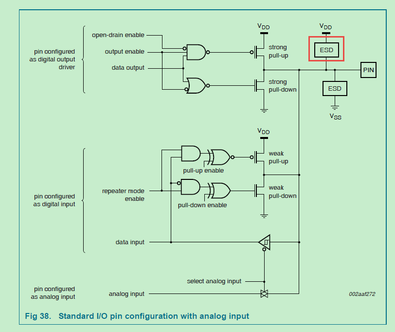
On normal inputs there is a diode to Vdd and a diode to Vss. So any input current goes into the power supply through these diodes. So if the microprocessor is consuming LESS than your input current, the current ends up in the power supply where a series-type voltage regulator can't do anything about it, and then you have an excessive power supply voltage.
The two diodes in series give you a PNPN junction structure just like a thyristor, so excessive current through either of the diodes is like the gate current of the thyristor which then latches ON.
5V tolerant inputs are different - I asked what the protection circuit consisted of and got no response (no surprise there!)
I think it must be like a zener, but I don't know for certain, so I would be much happier using my own external zener.
I suppose you could use the input pull-down option to cancel your input current, but as that can vary from 10uA to 100uA the input voltage could end up anywhere, so that's not a great idea either.
If you do use an external zener, don't forget that the external voltage must get below 1V for it to be certain to read a logic zero.
If you know the possible range of your external voltage, then it is best to use a potential divider. That way you can be certain of your logic 1 and logic 0 thresholds. So it's cost you ONE RESISTOR!
The current through the divider will be determined by the pin input capacitance and the speed that you require.
Maybe you need a capacitor in parallel to remove any transients?
If you don't know your external voltage, but just know that it's larger than 5V, then it will require a little more thought; and perhaps more than one extra component!
- Mark as New
- Bookmark
- Subscribe
- Mute
- Subscribe to RSS Feed
- Permalink
- Report Inappropriate Content
Dear Ian,
if You build 100000+ units and one part cost about 1~2 ct (material, placing, soldering, testing ...) - it makes sense to look which parts are really required.
Regarding the 5V inputs I also guess that there is a zener (3.6V) used - because the max. input voltage @ Vdd=0V is 3.6V. But I hope we will get a answer whats really behind it (Or which capabilities the circuit has).
Andreas
- Mark as New
- Bookmark
- Subscribe
- Mute
- Subscribe to RSS Feed
- Permalink
- Report Inappropriate Content
Hi,
1. Is it allowed to drive the input with a current source and let the protection circuit "adjust" the voltage?
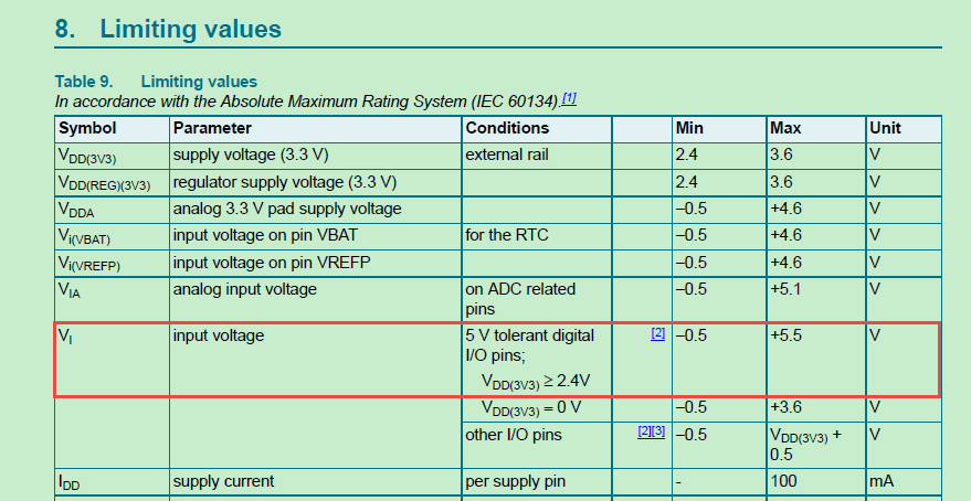
TS: From LPC1778 datasheet, the 5V tolerance I/O Max. input voltage is +5.5V with below table:
There doesn't allow the 5V tolerance I/O pin input voltage more than +5.5V.
2. The I/O latch-up current 100mA is the ultimate I/O pin current for very short time. If there I/O pin current exceed 100mA for a very short time, the LPC1778 chip will be damaged.
Thank you for the attention.
Have a great day,
Mike
-----------------------------------------------------------------------------------------------------------------------
Note: If this post answers your question, please click the Correct Answer button. Thank you!
-----------------------------------------------------------------------------------------------------------------------
- Mark as New
- Bookmark
- Subscribe
- Mute
- Subscribe to RSS Feed
- Permalink
- Report Inappropriate Content
Hi Mike,
thank You for the fast response!
1. So the protection circuits aren't able to sink a current? At my point of view the max. V_I voltages are these Voltages, where the protection circuit isn't working (sinking current). If the V_I increases above this value somewhere the protection circuit begins to work and draws current - but wasn't damage. If my point of view is correct - which is the maximum allowed current?
2. What is the source/the cause of the latch up current?
Regards and have also a nice day,
Andreas
- Mark as New
- Bookmark
- Subscribe
- Mute
- Subscribe to RSS Feed
- Permalink
- Report Inappropriate Content
Hi Andreas,
1. For LPC1778 datasheet doesn't provide the DC injection current value, I need to check with LPC product team about that parameter. With DC injection current value, we could calculate the serial resistor value to protect the diodes heating in pads. I will let you know when there with any comments.
2. A common cause of latch-up is a positive or negative voltage spike on an input or output pin of a digital chip that exceeds the rail voltage by more than a diode drop(such as: ESD issue). Another cause is the supply voltage exceeding the absolute maximum rating, often from a transient spike in the power supply( such as: I/O input voltage exceed VDD-GND range).
Have a great day,
Mike
-----------------------------------------------------------------------------------------------------------------------
Note: If this post answers your question, please click the Correct Answer button. Thank you!
-----------------------------------------------------------------------------------------------------------------------
- Mark as New
- Bookmark
- Subscribe
- Mute
- Subscribe to RSS Feed
- Permalink
- Report Inappropriate Content
Hi Mike,
=>1: Thank You for passing my question to the LPC product team.
=>2: The latch up effect is known, but I have no idea until now what the value really means and what it deals with my circuit around the LPC.
Have a nice week,
Andreas

