- NXP Forums
- Product Forums
- General Purpose MicrocontrollersGeneral Purpose Microcontrollers
- i.MX Forumsi.MX Forums
- QorIQ Processing PlatformsQorIQ Processing Platforms
- Identification and SecurityIdentification and Security
- Power ManagementPower Management
- MCX Microcontrollers
- S32G
- S32K
- S32V
- MPC5xxx
- Other NXP Products
- Wireless Connectivity
- S12 / MagniV Microcontrollers
- Powertrain and Electrification Analog Drivers
- Sensors
- Vybrid Processors
- Digital Signal Controllers
- 8-bit Microcontrollers
- ColdFire/68K Microcontrollers and Processors
- PowerQUICC Processors
- OSBDM and TBDML
-
- Solution Forums
- Software Forums
- MCUXpresso Software and ToolsMCUXpresso Software and Tools
- CodeWarriorCodeWarrior
- MQX Software SolutionsMQX Software Solutions
- Model-Based Design Toolbox (MBDT)Model-Based Design Toolbox (MBDT)
- FreeMASTER
- eIQ Machine Learning Software
- Embedded Software and Tools Clinic
- S32 SDK
- S32 Design Studio
- Vigiles
- GUI Guider
- Zephyr Project
- Voice Technology
- Application Software Packs
- Secure Provisioning SDK (SPSDK)
- Processor Expert Software
-
- Topics
- Mobile Robotics - Drones and RoversMobile Robotics - Drones and Rovers
- NXP Training ContentNXP Training Content
- University ProgramsUniversity Programs
- Rapid IoT
- NXP Designs
- SafeAssure-Community
- OSS Security & Maintenance
- Using Our Community
-
-
- Home
- :
- i.MX Forums
- :
- i.MX Processors
- :
- i.MX7Dual high-speed ADC sampling
i.MX7Dual high-speed ADC sampling
- Subscribe to RSS Feed
- Mark Topic as New
- Mark Topic as Read
- Float this Topic for Current User
- Bookmark
- Subscribe
- Mute
- Printer Friendly Page
i.MX7Dual high-speed ADC sampling
- Mark as New
- Bookmark
- Subscribe
- Mute
- Subscribe to RSS Feed
- Permalink
- Report Inappropriate Content
Hello,
[Edited to add new information.]
I have an i.MX7Dual Sabre SD development board and I would like to develop a test application that performs high-speed (1 Msample/sec) sampling of the two ADC blocks on the M4 as a bare metal application. I have read through Ch. 14 of the reference manual and reviewed the adc_imx7d example in the FreeRTOS BSP, but I still have several questions:
- [A previous version of this question asked about multiple channels, but I since realized that it would be better to use a single channel for both ADCs, so I have removed the channel-related questions.]
- The manual briefly mentions a DMA FIFO for the ADCs, but it does not address how to use DMA with the ADCs. Similarly, the FreeRTOS BSP ADC driver does not support DMA and neither does the Linux kernel driver in the forked 4.1.x kernel series. Is there some other documentation or source of examples that can provide details on using DMA with A/D conversion?
- One motivation for using the FIFO mechanism is that it provides feedback for FIFO over/underruns. If not using FIFO/DMA, is there any way to determine if we are dropping samples? I believe that the i.MX6 SoCs had a flag to control whether new samples overwrote previous samples or were discarded in the case that the conversion complete flag was still set from a previous conversion, but the i.MX7 manual does not seem to address the possibility of overruns, other than when using the FIFO with DMA.
- What constitutes a conversion timeout? I have developed a sample bare metal application and have confirmed that conversion overruns do not set the timeout flag, so from what I can tell, there is no way to determine if samples have been dropped/missed.
- All of the MX7D SabreSD documentation indicates that the M4 runs at "up to 200 MHz". It appears based on the BSP and the values reported from the cycle counter that the M4 is actually running at 240 MHz (e.g. see the SystemCoreClock variable in system_MCIMX7D_M4.c from the BSP).
- I believe there may be a bug in the ADC driver for the FreeRTOS BSP. In the function ADC_SetConvertRate() from adc_imx7d.c, the quotient sampleRate/convertRate is written to the CHA_TIMER field of the CFG1 register, but according to the documentation this yields a conversion rate of (CHA_TIMER+1)*sampleRate. Thus, for matched values, we want CHA_TIMER=0 rather than CHA_TIMER=1; presumably we need to subtract 1 from the quotient prior to writing it to CHA_TIMER.
I have developed a bare-metal application running on the M4 that samples both ADCs in continuous mode using matched-priority interrupts. I also record the cycle counter immediately after reading the ADC value. I get stable results when only managing a single ADC (cycle counts reliably in the range 238-242 cycles, which is consistent with a 240 MHz clock and 1 MSPS sampling). However, with both ADC blocks running, I get some timing anomalies. For example, I see the following with a single ADC:
conv=2608 cyc= 5291581 diff=241
conv=2576 cyc= 5291820 diff=239
conv=2549 cyc= 5292062 diff=242
conv=2505 cyc= 5292300 diff=238
conv=2475 cyc= 5292542 diff=242
conv=2429 cyc= 5292780 diff=238
conv=2399 cyc= 5293022 diff=242
conv=2371 cyc= 5293260 diff=238
and this with two:
conv=2399 cyc= 5294669 diff=460 conv=3060 cyc= 5295358 diff=458
conv=2339 cyc= 5295131 diff=462 conv=2979 cyc= 5295821 diff=463
conv=2294 cyc= 5295590 diff=459 conv=2864 cyc= 5296279 diff=458
conv=2263 cyc= 5296048 diff=458 conv=2792 cyc= 5296742 diff=463
conv=2204 cyc= 5296510 diff=462 conv=2757 cyc= 5297200 diff=458
conv=2170 cyc= 5296969 diff=459 conv=2514 cyc= 5299500 diff=2300
where conv is the raw value from the ADC, cyc is the cycle counter, and diff is the difference between cycle counters for the same block. I fill up a fixed-sized buffer and then stop the ADCs to print the results, so there are no debugging print statements while processing. The conversions seem to be running at roughly half-rate with both blocks enabled. In addition, I seem to drop a lot of samples from ADC2 intermittently (i.e. the diff=2300 above). Does anyone know why this is the case?
More generally, does anyone have any recommendations for reliably sampling both ADCs at 1 MSPS without dropping samples? Or is this task just not suited to this SoC?
Regards,
Thomas
- Mark as New
- Bookmark
- Subscribe
- Mute
- Subscribe to RSS Feed
- Permalink
- Report Inappropriate Content
Hi Thomas,
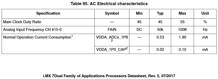
Additionally, if you refer to Table 95 “AC Electrical characteristics” of the i.MX7D datasheet, it is indicated that the maximum Analog Input Frequency is 100KHz:
Hope this will be useful for you.
Best regards!
/Carlos
-----------------------------------------------------------------------------------------------------------------------
Note: If this post answers your question, please click the Correct Answer button. Thank you!
-----------------------------------------------------------------------------------------------------------------------
- Mark as New
- Bookmark
- Subscribe
- Mute
- Subscribe to RSS Feed
- Permalink
- Report Inappropriate Content
That is the analog input to the ADC, not the conversion rate.
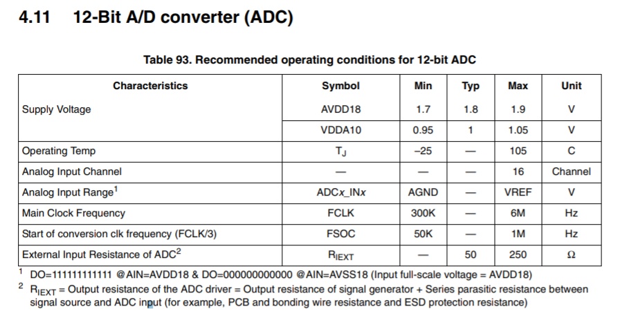
Table 93. states the maximum Start of conversion clk frequency is 1MHz
- Mark as New
- Bookmark
- Subscribe
- Mute
- Subscribe to RSS Feed
- Permalink
- Report Inappropriate Content
Recommendation for running both ADCs at 1MSPS is to use the DMA.
I have not worked with this particular processor but generally you program the ADC to generate a DMA request when conversion is done and then you program the DMA to transfer from peripheral(ADC) to memory(RAM). Usually you program the DMA to automatically increase the address for each transfer and set a number of samples to transfer and stop after doing that number of transfers.
Most of the problems you describe when using both ADCs seem to be because it does not have enough time to process 2 interrupts per microsecond. At 240 MHz CPU clock, and 1MSPS conversion rate gives you 240 cycles to handle the interrupt ( interrupt latency, push all registers to stack, service interrupt, pull registers from stack -- full context switch if using OS). When you use 2 ADCs at this rate you only have 120 cycles to do all that and apparently you need close to 240 cycles for it. So it is impossible to do it using interrupts.
You can try slowing down your ADC (try 100KSPS) and it will probably work as you expect. Then keep increasing the ADC rate and I expect that somewhere around 500KSPS it will start having trouble.
Also look at the registers, there is a "DMA FIFO Overrun" and a "FIFO Overrun"
I am not sure but I think a "conversion timeout" occurs if you try to trigger a conversion when a previous conversion is not done(conversion rate is too fast for ADC).
Hope this helps
- Mark as New
- Bookmark
- Subscribe
- Mute
- Subscribe to RSS Feed
- Permalink
- Report Inappropriate Content
Hi Raymundo,
Thank you for the helpful information! I would like to use DMA, but I am not sure how to program it based on the information in the reference manual. I did see the DMA registers (e.g. a bit to enable DMA, a DMA FIFO register, the under/overflow flags you mentioned, watermark levels, etc.), but I have no idea how to actually program the transfers and monitor their progress. For example, the DMA FIFO is 32x32 bits based on the documentation, but the DMA FIFO register is just a single word, so it seems to reference status for a FIFO that resides somewhere else in memory. However, I did not see any indication of how to point the DMA engine to an address storing the FIFO. There is a DMA_FIFO_DAT word that seemingly stores two 12-bit samples, but again it is just a 32 bit word, not a 32x32 bit block of data as indicated in the documentation.
Should I be looking elsewhere for documentation for using DMA with the ADC? Perhaps these fields are all standard and their use is documented elsewhere. I looked a bit through the SDMA chapter in the reference manual, but I don't know if I have to write a custom SDMA script for this.
Thanks for your help,
Thomas
- Mark as New
- Bookmark
- Subscribe
- Mute
- Subscribe to RSS Feed
- Permalink
- Report Inappropriate Content
As I mentioned I have not worked on this particular processor. My experience with something similar to this is with the ADCHS in the LPC4370, but I'll try to answer your questions.
First, the FIFO is exactly that, a FIFO(First In First Out). This one contains 32 words. When you retrieve a value it will retrieve the oldest value and then make the next oldest value available for next time you read the FIFO, so the address for it does not need to be changed.
Most DMAs will have one of two ways to handle this.
1. You specify you want the DMA transfer "Peripheral to Memory", "Memory to Peripheral" or "Memory to Memory". In this case the Peripheral will always be accessed at the specified address (the FIFO address in this case) and Memory will be automatically increased by the transfer width.
2. You can specify a transfer "Address1 to Address2" and also specify whether Address1 and/or Address2 remain fixed or are incremented automatically by the transfer width.
You can usually check for a "DMA complete" flag or use the "DMA Complete" interrupt to know when all the samples have been transferred.
Maybe you can find (or someone from NXP can help you find) some examples for this particular processor/DMA.

