- NXP Forums
- Product Forums
- General Purpose MicrocontrollersGeneral Purpose Microcontrollers
- i.MX Forumsi.MX Forums
- QorIQ Processing PlatformsQorIQ Processing Platforms
- Identification and SecurityIdentification and Security
- Power ManagementPower Management
- MCX Microcontrollers
- S32G
- S32K
- S32V
- MPC5xxx
- Other NXP Products
- Wireless Connectivity
- S12 / MagniV Microcontrollers
- Powertrain and Electrification Analog Drivers
- Sensors
- Vybrid Processors
- Digital Signal Controllers
- 8-bit Microcontrollers
- ColdFire/68K Microcontrollers and Processors
- PowerQUICC Processors
- OSBDM and TBDML
-
- Solution Forums
- Software Forums
- MCUXpresso Software and ToolsMCUXpresso Software and Tools
- CodeWarriorCodeWarrior
- MQX Software SolutionsMQX Software Solutions
- Model-Based Design Toolbox (MBDT)Model-Based Design Toolbox (MBDT)
- FreeMASTER
- eIQ Machine Learning Software
- Embedded Software and Tools Clinic
- S32 SDK
- S32 Design Studio
- Vigiles
- GUI Guider
- Zephyr Project
- Voice Technology
- Application Software Packs
- Secure Provisioning SDK (SPSDK)
- Processor Expert Software
-
- Topics
- Mobile Robotics - Drones and RoversMobile Robotics - Drones and Rovers
- NXP Training ContentNXP Training Content
- University ProgramsUniversity Programs
- Rapid IoT
- NXP Designs
- SafeAssure-Community
- OSS Security & Maintenance
- Using Our Community
-
-
- Home
- :
- General Purpose Microcontrollers
- :
- LPC Microcontrollers
- :
- LPC1788 from scratch, minimum circuit?
LPC1788 from scratch, minimum circuit?
- Subscribe to RSS Feed
- Mark Topic as New
- Mark Topic as Read
- Float this Topic for Current User
- Bookmark
- Subscribe
- Mute
- Printer Friendly Page
LPC1788 from scratch, minimum circuit?
- Mark as New
- Bookmark
- Subscribe
- Mute
- Subscribe to RSS Feed
- Permalink
- Report Inappropriate Content
Had a quick look through the datasheet and user manual for the LPC1788 but didn't see a basic circuit to get it up and running. I did see the crystal circuit in that chapter and the debug options in another chapter but where is the power? Section 3.12 "Power control" of the user manual hasn't got a single graphic. Chapter 6 "Pin Configuration" doesn't seem to mention power lines just I/O.
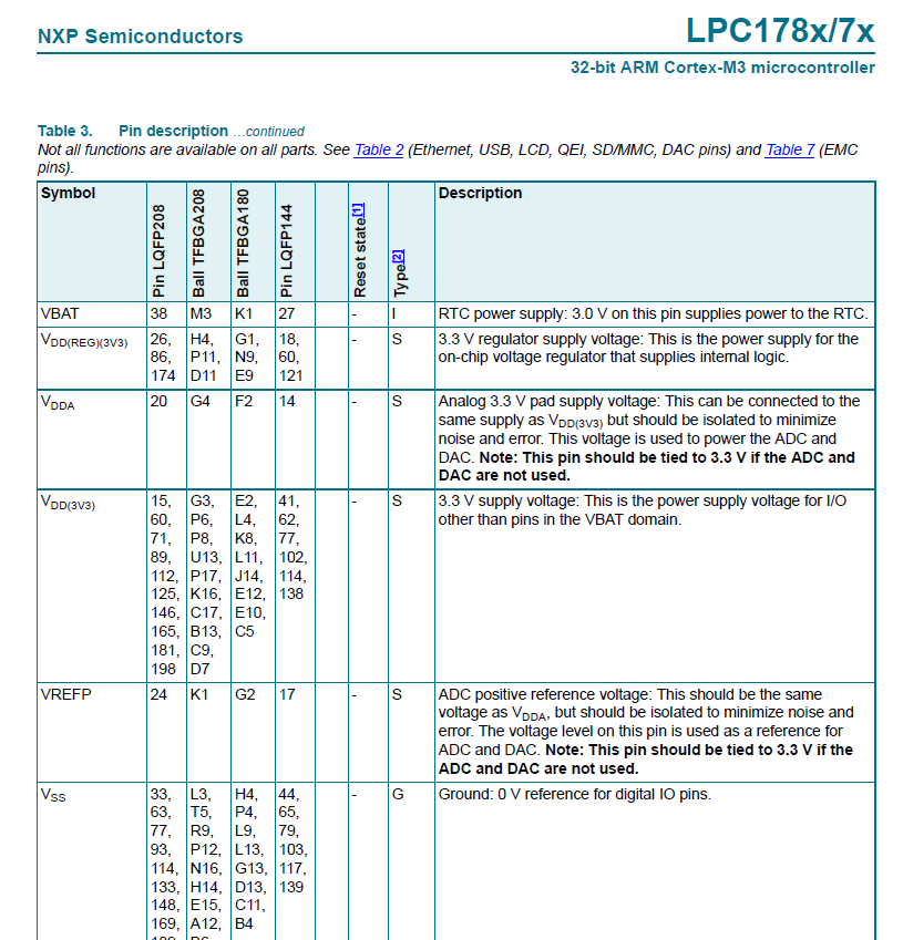
Section 6 of the Datasheet does list the Power pins. So for the LQFP144 Vdd is pins 41,62,77,102,114,138 listed as the 3.3v power supply. No mention of bypass caps. Does that mean no Caps? Certainly save on the parts count.
What have I missed? Looked at application notes listed on web site. Nothing relevant. Lots of information on the various peripherals but if I can't actually power up the device all that peripheral information is wasted on me. Maybe I'm showing my ignorance and everybody knows the required circuit.
- Mark as New
- Bookmark
- Subscribe
- Mute
- Subscribe to RSS Feed
- Permalink
- Report Inappropriate Content
All the information is in the datasheet (mine is from April 26 2016).
None of the detailed hardware info is in the users manual, this concentrates on the peripherals and the usage of these.
Look in chapter 6, table 3 of the datasheet. All pins are shown and all the power pins are also there. It is also recommended to study designs from other board providers to get an idea of whats needed. All the information is "out there" I can guarantee you :smileywink:
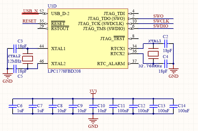
This is the debug connections I use (for a 208 pin package), "USB_N" is for my USB connection so disregard that one:
The RTC xtal and caps are not needed for a "bare minimum" circuit.
Below is the decoupling caps I use on most of my 177x/178x designs, have worked perfect so far.
- Mark as New
- Bookmark
- Subscribe
- Mute
- Subscribe to RSS Feed
- Permalink
- Report Inappropriate Content
Thanks a million for your response. I'm maybe too used to having access to required information from the provider of a chip. Thanks for your suggested circuit as well, but that to me seems a bit vague. I'm a SW engineer so I'm coming at this from that perspective. Other uC's I've put on a PCB suggest both minimum circuit, the bypass caps required, and a suggested placement of those caps. Apparently from an electronic perspective the distance between the Cap and the uC can have some sort of effect on the device. The area around the uC can get a bit busy, there's a lot of connections in that area, and putting the bypass caps as far away as possible would suit me, but usually that's not considered a great design.
You're suggesting that to get information for an NXP LPC1788 that I pursue that with third party board providers. I'm a bit confused by that and wonder why they'd give me access to their information. I'm not their customer or even potential customer.
I have been over the table you suggested in the Datsheet and mentioned it in my original post. I have pin numbers for Vss and Vdd but no indication of anything other then numbers. I guess this is a community channel and I should really be opening a formal ticket with NXP to ask them for a response.
- Mark as New
- Bookmark
- Subscribe
- Mute
- Subscribe to RSS Feed
- Permalink
- Report Inappropriate Content
Google for "LPC1788 designs"...
Olimex, Embedded Artists, Future Designs Inc (FDI) and many other have documented their boards with both schematics and layout etc. There is a ton of info out there for grabs.
- Mark as New
- Bookmark
- Subscribe
- Mute
- Subscribe to RSS Feed
- Permalink
- Report Inappropriate Content
This must have either been a badly formed question, or I asked it in the wrong place. If anybody could suggest which is the problem I'll try to address that in order to get an answer. I would like to put the LPC1788 onto a PCB but in order to do that there is information required which I have been unable to find.

