- NXP Forums
- Product Forums
- General Purpose MicrocontrollersGeneral Purpose Microcontrollers
- i.MX Forumsi.MX Forums
- QorIQ Processing PlatformsQorIQ Processing Platforms
- Identification and SecurityIdentification and Security
- Power ManagementPower Management
- MCX Microcontrollers
- S32G
- S32K
- S32V
- MPC5xxx
- Other NXP Products
- Wireless Connectivity
- S12 / MagniV Microcontrollers
- Powertrain and Electrification Analog Drivers
- Sensors
- Vybrid Processors
- Digital Signal Controllers
- 8-bit Microcontrollers
- ColdFire/68K Microcontrollers and Processors
- PowerQUICC Processors
- OSBDM and TBDML
-
- Solution Forums
- Software Forums
- MCUXpresso Software and ToolsMCUXpresso Software and Tools
- CodeWarriorCodeWarrior
- MQX Software SolutionsMQX Software Solutions
- Model-Based Design Toolbox (MBDT)Model-Based Design Toolbox (MBDT)
- FreeMASTER
- eIQ Machine Learning Software
- Embedded Software and Tools Clinic
- S32 SDK
- S32 Design Studio
- Vigiles
- GUI Guider
- Zephyr Project
- Voice Technology
- Application Software Packs
- Secure Provisioning SDK (SPSDK)
- Processor Expert Software
-
- Topics
- Mobile Robotics - Drones and RoversMobile Robotics - Drones and Rovers
- NXP Training ContentNXP Training Content
- University ProgramsUniversity Programs
- Rapid IoT
- NXP Designs
- SafeAssure-Community
- OSS Security & Maintenance
- Using Our Community
-
-
- Home
- :
- i.MX Forums
- :
- i.MX Processors
- :
- iMAX6Q DRAM_D[0..63] & DDR3_SDRAM DQ[0..15] Pin Mapping
iMAX6Q DRAM_D[0..63] & DDR3_SDRAM DQ[0..15] Pin Mapping
- Subscribe to RSS Feed
- Mark Topic as New
- Mark Topic as Read
- Float this Topic for Current User
- Bookmark
- Subscribe
- Mute
- Printer Friendly Page
iMAX6Q DRAM_D[0..63] & DDR3_SDRAM DQ[0..15] Pin Mapping
- Mark as New
- Bookmark
- Subscribe
- Mute
- Subscribe to RSS Feed
- Permalink
- Report Inappropriate Content
Dear All,
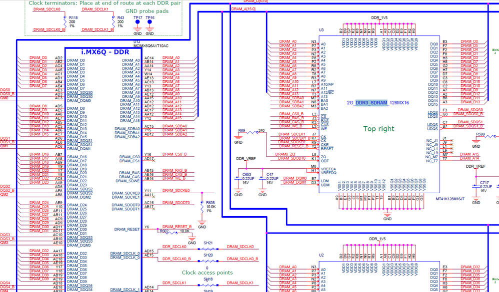
I am referring to the following Sabre SD DDR RAM schematic and I need to know how to configure the pin map of the processor and RAM. (The order of the DRAM_D[0 to 63] with DQ[0 to 15] )
MT41K128M16JT RAM has used in Sabre SD board and the pins have connected as follows.
DRAM_D0 >> DQ0
DRAM_D1 >> DQ3
DRAM_D2 >> DQ6
DRAM_D3 >> DQ4
How the above bit pattern select according to each RAM. Do we have any method to know which DQ pin will connect with DRAM pin ?
Regards,
Peter.
- Mark as New
- Bookmark
- Subscribe
- Mute
- Subscribe to RSS Feed
- Permalink
- Report Inappropriate Content
Hi Peter
please look at sect.3.6.1 Swapping data lines i.MX6 System Development User’s Guide
http://cache.freescale.com/files/32bit/doc/user_guide/IMX6DQ6SDLHDG.pdf
Best regards
igor
-----------------------------------------------------------------------------------------------------------------------
Note: If this post answers your question, please click the Correct Answer button. Thank you!
-----------------------------------------------------------------------------------------------------------------------
- Mark as New
- Bookmark
- Subscribe
- Mute
- Subscribe to RSS Feed
- Permalink
- Report Inappropriate Content
Dear #igorpadykov
Thank you for the reply and now I can understand the swapping of the data lines.
"Hardware write leveling – lowest order bit within byte lane must remain on lowest order bit of lane by JEDEC compliance (see the “Write Leveling” section in JESD79-3E) — D0, D8, D16, D24, D32, D40, D48, and D56 are fixed — Other data lines free to swap within byte lane."
But could you please tell me how this happen ?
In first data set D0 connect to DQ0 and in third data set D16 connect to DQ8(NOT DQ0) why is that ?
Is this a matter of LDM and UDM bit selection of DRAM_DQM ?
Regards,
Peter.
- Mark as New
- Bookmark
- Subscribe
- Mute
- Subscribe to RSS Feed
- Permalink
- Report Inappropriate Content
Hi Peter
right, bits may be swapped within byte group, important LDM, UDM selections.
Best regards
igor
- Mark as New
- Bookmark
- Subscribe
- Mute
- Subscribe to RSS Feed
- Permalink
- Report Inappropriate Content
Hi #igorpadykov,
But could you please tell me how this happen ?
In first data set D0 connect to DQ0 and in third data set D16 connect to DQ8(NOT DQ0) why is that ?
Is this a matter of LDM and UDM bit selection of DRAM_DQM ?
How do we select LDM and UDM ? How to swap DQ according to LDM UDM selection ?
Regards,
Peter.
- Mark as New
- Bookmark
- Subscribe
- Mute
- Subscribe to RSS Feed
- Permalink
- Report Inappropriate Content
Hi
what do you mean by
" third data set D16 connect to DQ8(NOT DQ0) why is that ? "
data bits can be swapped within byte only.
Best regards
igor
