
- NXP Forums
- Product Forums
- General Purpose MicrocontrollersGeneral Purpose Microcontrollers
- i.MX Forumsi.MX Forums
- QorIQ Processing PlatformsQorIQ Processing Platforms
- Identification and SecurityIdentification and Security
- Power ManagementPower Management
- MCX Microcontrollers
- S32G
- S32K
- S32V
- MPC5xxx
- Other NXP Products
- Wireless Connectivity
- S12 / MagniV Microcontrollers
- Powertrain and Electrification Analog Drivers
- Sensors
- Vybrid Processors
- Digital Signal Controllers
- 8-bit Microcontrollers
- ColdFire/68K Microcontrollers and Processors
- PowerQUICC Processors
- OSBDM and TBDML
-
- Solution Forums
- Software Forums
- MCUXpresso Software and ToolsMCUXpresso Software and Tools
- CodeWarriorCodeWarrior
- MQX Software SolutionsMQX Software Solutions
- Model-Based Design Toolbox (MBDT)Model-Based Design Toolbox (MBDT)
- FreeMASTER
- eIQ Machine Learning Software
- Embedded Software and Tools Clinic
- S32 SDK
- S32 Design Studio
- Vigiles
- GUI Guider
- Zephyr Project
- Voice Technology
- Application Software Packs
- Secure Provisioning SDK (SPSDK)
- Processor Expert Software
-
- Topics
- Mobile Robotics - Drones and RoversMobile Robotics - Drones and Rovers
- NXP Training ContentNXP Training Content
- University ProgramsUniversity Programs
- Rapid IoT
- NXP Designs
- SafeAssure-Community
- OSS Security & Maintenance
- Using Our Community
-
- Cloud Lab Forums
-
- Home
- :
- Product Forums
- :
- S12 / MagniV Microcontrollers
- :
- What is the expected status (High/Low) of Port P and S pin when the S12ZVL comes out of reset?
What is the expected status (High/Low) of Port P and S pin when the S12ZVL comes out of reset?
- Subscribe to RSS Feed
- Mark Topic as New
- Mark Topic as Read
- Float this Topic for Current User
- Bookmark
- Subscribe
- Mute
- Printer Friendly Page
- Mark as New
- Bookmark
- Subscribe
- Mute
- Subscribe to RSS Feed
- Permalink
- Report Inappropriate Content
What is the expected status (High/Low) of Port P and S pin when the S12ZVL comes out of reset? I am testing the controller in and around the Low Voltage Assert (2.95V) to Low Voltage De-assert (3.13V) range. I see that when supply voltage exceeds 3.13V, Port S and P go high momentarily and automatically come down. I am using these port pins as output and they have been initialized to 0 in the code.
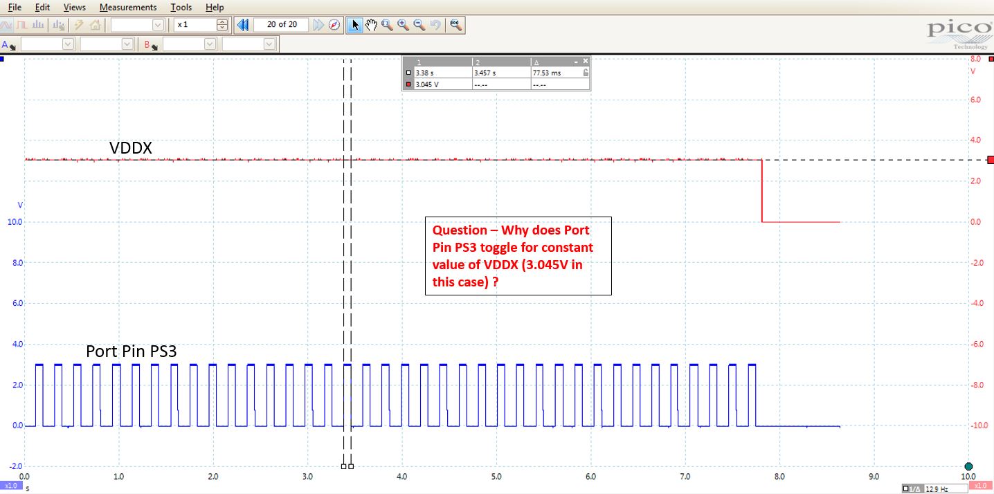
Additionally I also observe that at for Supply Voltage between 2.95V - 3.13V, the pin PS3 toggles constantly. What could be the reason for this behavior?
Solved! Go to Solution.
- Mark as New
- Bookmark
- Subscribe
- Mute
- Subscribe to RSS Feed
- Permalink
- Report Inappropriate Content
Hi Kumar,
Please look at Table 1-6. Pin Summary in RM.
This table defines default state of pin right after reset.
Both P and S ports are defined as Off. It means that they are configured as a digital input (that is common for all GPIO pins) without internal pull-up/down = floating input.
So, from this point of view, the voltage level at these pins will be strongly influenced by connected external devices at these pins. If you need manage, that these pins will have specific voltage level when MCU reset and prior output is enabled, you must use an external pull-up or pull-down.
Note: I would like to recommend do not leave unused GPIO pin floating. This may cause higher power consumption when pin input voltage is in the linear area near to VDDX/2. This is not valid for port AD until we enable digital input pin buffer in DIENAD register.
You didn‘t specify how PS3 pin is configured by your code. This toggling may be caused by two effects.
When PS3 is in the default state (floating input), the result voltage level is given by the combination of MCU and test equipment leakage currents.
The voltage 3.045V is right at edge of Low Voltage Interrupt. So, I suppose, that MCU may periodically enter and leave reset state and you simply see Low Voltage assert and deassert hysteresis. These minimal waves at power supply may be caused by simple charging/discharging blocking capacitors (The MCU have probably higher power consumption in a run mode in compare with reset state).
I hope it helps you.
Have a great day,
Radek
-----------------------------------------------------------------------------------------------------------------------
Note: If this post answers your question, please click the Correct Answer button. Thank you!
-----------------------------------------------------------------------------------------------------------------------
- Mark as New
- Bookmark
- Subscribe
- Mute
- Subscribe to RSS Feed
- Permalink
- Report Inappropriate Content
Hi Radek,
Thanks for the reply, it helped me narrow down to the problem. I have configured the pin PS3 as output. You are right, I need to externally pull-up or pull-down to make my circuit work the way I want.
Thanks again.
Kumar