- NXP Forums
- Product Forums
- General Purpose MicrocontrollersGeneral Purpose Microcontrollers
- i.MX Forumsi.MX Forums
- QorIQ Processing PlatformsQorIQ Processing Platforms
- Identification and SecurityIdentification and Security
- Power ManagementPower Management
- MCX Microcontrollers
- S32G
- S32K
- S32V
- MPC5xxx
- Other NXP Products
- Wireless Connectivity
- S12 / MagniV Microcontrollers
- Powertrain and Electrification Analog Drivers
- Sensors
- Vybrid Processors
- Digital Signal Controllers
- 8-bit Microcontrollers
- ColdFire/68K Microcontrollers and Processors
- PowerQUICC Processors
- OSBDM and TBDML
-
- Solution Forums
- Software Forums
- MCUXpresso Software and ToolsMCUXpresso Software and Tools
- CodeWarriorCodeWarrior
- MQX Software SolutionsMQX Software Solutions
- Model-Based Design Toolbox (MBDT)Model-Based Design Toolbox (MBDT)
- FreeMASTER
- eIQ Machine Learning Software
- Embedded Software and Tools Clinic
- S32 SDK
- S32 Design Studio
- Vigiles
- GUI Guider
- Zephyr Project
- Voice Technology
- Application Software Packs
- Secure Provisioning SDK (SPSDK)
- Processor Expert Software
-
- Topics
- Mobile Robotics - Drones and RoversMobile Robotics - Drones and Rovers
- NXP Training ContentNXP Training Content
- University ProgramsUniversity Programs
- Rapid IoT
- NXP Designs
- SafeAssure-Community
- OSS Security & Maintenance
- Using Our Community
-
-
- Home
- :
- Identification and Security
- :
- NFC
- :
- About processing of unused pins in PN532
About processing of unused pins in PN532
- Subscribe to RSS Feed
- Mark Topic as New
- Mark Topic as Read
- Float this Topic for Current User
- Bookmark
- Subscribe
- Mute
- Printer Friendly Page
- Mark as New
- Bookmark
- Subscribe
- Mute
- Subscribe to RSS Feed
- Permalink
- Report Inappropriate Content
I am designing NFC product using PN532.
There are some unused pins.
Could you tell me the processing of un used pins?
Unsed pins are below.
2 , 12 ,13 , 24 , 29 ~ 37
Solved! Go to Solution.
- Mark as New
- Bookmark
- Subscribe
- Mute
- Subscribe to RSS Feed
- Permalink
- Report Inappropriate Content
Hello 利幸 酒井 ,
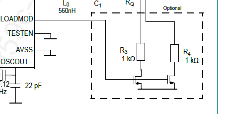
1. PIN2---LOADMOD
Accroding to datasheet, Fig 51. Application diagram of PN532,
This part of circuit is optional, so LOADMOD signal can be floating.
2. PIN12---AUX1 ; PIN13---AUX2
These 2 PIN should be connected Test Points.
3. PIN24---UART_RX ; PIN31---UART_TX
These 2 PINs are signal for debug UART.
-- PIN24 should be connected to GND or pull it up to High with 4.7K/10K resistor.
---PIN31 can be floating.
4. PIN27,28,29,30
These 4 PINs are signal for Host Interface: SPI / i2c / High Speed UART. I don't kown if you don't use them, how will you run software for PN532? because it means you don't want to use MCU or processor.
----Input signals should be connected to GND or pull it up to High with 4.7K/10K resistor.
---output signals can be floating.
5. PIN32 & PIN33
These 2 PINs are both interrupt sources, used send interrupt to MCU.they can also be floating if you don't need them, but are you really sure you don't need them?
6. PIN34 ~ PIN37
This is interface for Secure IC, if you don't need them, PIN37(SVDD) can be conntected a 0.1uF capacitor close to PN532, PIN36 should be connected to GND or pull it up to High with 4.7K/10K resistor, other 2 PINs can be floating.
Regards,
Weidong
