- NXP Forums
- Product Forums
- General Purpose MicrocontrollersGeneral Purpose Microcontrollers
- i.MX Forumsi.MX Forums
- QorIQ Processing PlatformsQorIQ Processing Platforms
- Identification and SecurityIdentification and Security
- Power ManagementPower Management
- MCX Microcontrollers
- S32G
- S32K
- S32V
- MPC5xxx
- Other NXP Products
- Wireless Connectivity
- S12 / MagniV Microcontrollers
- Powertrain and Electrification Analog Drivers
- Sensors
- Vybrid Processors
- Digital Signal Controllers
- 8-bit Microcontrollers
- ColdFire/68K Microcontrollers and Processors
- PowerQUICC Processors
- OSBDM and TBDML
-
- Solution Forums
- Software Forums
- MCUXpresso Software and ToolsMCUXpresso Software and Tools
- CodeWarriorCodeWarrior
- MQX Software SolutionsMQX Software Solutions
- Model-Based Design Toolbox (MBDT)Model-Based Design Toolbox (MBDT)
- FreeMASTER
- eIQ Machine Learning Software
- Embedded Software and Tools Clinic
- S32 SDK
- S32 Design Studio
- Vigiles
- GUI Guider
- Zephyr Project
- Voice Technology
- Application Software Packs
- Secure Provisioning SDK (SPSDK)
- Processor Expert Software
-
- Topics
- Mobile Robotics - Drones and RoversMobile Robotics - Drones and Rovers
- NXP Training ContentNXP Training Content
- University ProgramsUniversity Programs
- Rapid IoT
- NXP Designs
- SafeAssure-Community
- OSS Security & Maintenance
- Using Our Community
-
-
- Home
- :
- i.MX Forums
- :
- i.MX Processors
- :
- About detailed explanation of CKExDESKEWCODE field for i.MX7
About detailed explanation of CKExDESKEWCODE field for i.MX7
- Subscribe to RSS Feed
- Mark Topic as New
- Mark Topic as Read
- Float this Topic for Current User
- Bookmark
- Subscribe
- Mute
- Printer Friendly Page
About detailed explanation of CKExDESKEWCODE field for i.MX7
- Mark as New
- Bookmark
- Subscribe
- Mute
- Subscribe to RSS Feed
- Permalink
- Report Inappropriate Content
Dear all,
We connect LPDDR2 to i.MX7Solo.
LPDDR2 is 400MHz operation.
We want to delay CKE signal for 2nsec.
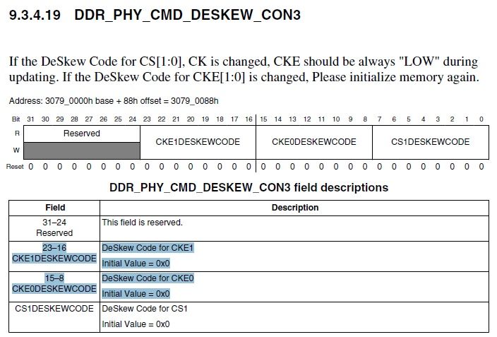
We refer to CKExDESKEWCODE field of the DDR_PHY_CMD_DESKEW_CON3 register.
However, we do not know what kind of value we should set.
What kind of value should we set for Delay of 2nsec?
Best Regards,
Yuuki
- Mark as New
- Bookmark
- Subscribe
- Mute
- Subscribe to RSS Feed
- Permalink
- Report Inappropriate Content
Hello Yuuki,
I'm investigating since there is no much detailed information on the documentation. I'll let you know as soon as I have more information.
Regards,
- Mark as New
- Bookmark
- Subscribe
- Mute
- Subscribe to RSS Feed
- Permalink
- Report Inappropriate Content
Dear gusarambula-san,
Thank you for a quick response.
I wait for information from you.
Best Regards,
Yuuki
- Mark as New
- Bookmark
- Subscribe
- Mute
- Subscribe to RSS Feed
- Permalink
- Report Inappropriate Content
Hello Yuuki-San,
I’ve received the following information:
One delay value in this register is ~16.3 picoseconds. This is equivalent to tFS (Fine Step delay). This is a fixed value that does not vary with DDR clock frequency. The register field values of 0x00 - 0x08 add no delay. For this field, 0x08 is effectively the zero starting point. Every setting above 0x08 adds one tFS delay. For example, a value of 0x12 adds 10*tFS or 163 picoseconds of delay.
The register field will add a maximum of 32 delay elements. Therefore, the maximum setting of 0x28 will add 32*16.3 picoseconds delay, or 522 picoseconds. Any value above 0x28 adds no further delay, so 2 nanoseconds is not possible.
It is also not recommended to delay CKE by a full clock cycle (or 80%). The CKE signal is an integral part of the CA signals that go to the LPDDR2 memory. If the CKE signal is delayed by a clock cycle the LPDDR2 memory will decode the CA command incorrectly and the LPDDR2 will not operate. If the problem is that the CKE signal does not rise fast enough to meet tISCKE requirements is this issue what would need to be addressed.
The Reference Manual does report that CA[9:0] DeSkew should be set to 0x60 for low frequency operatons. CKE pads are different than other pads.
The CKE signal drive strength can be increased in field DRVDS_CON0.CACKEDRVRDS 0x3079009C[8:6]. Setting of 0x3 is maximum. If there is a pull down resistor on CKE, removing the resitor will also help.
I hope this information helps!
Regards,
