- NXP Forums
- Product Forums
- General Purpose MicrocontrollersGeneral Purpose Microcontrollers
- i.MX Forumsi.MX Forums
- QorIQ Processing PlatformsQorIQ Processing Platforms
- Identification and SecurityIdentification and Security
- Power ManagementPower Management
- MCX Microcontrollers
- S32G
- S32K
- S32V
- MPC5xxx
- Other NXP Products
- Wireless Connectivity
- S12 / MagniV Microcontrollers
- Powertrain and Electrification Analog Drivers
- Sensors
- Vybrid Processors
- Digital Signal Controllers
- 8-bit Microcontrollers
- ColdFire/68K Microcontrollers and Processors
- PowerQUICC Processors
- OSBDM and TBDML
-
- Solution Forums
- Software Forums
- MCUXpresso Software and ToolsMCUXpresso Software and Tools
- CodeWarriorCodeWarrior
- MQX Software SolutionsMQX Software Solutions
- Model-Based Design Toolbox (MBDT)Model-Based Design Toolbox (MBDT)
- FreeMASTER
- eIQ Machine Learning Software
- Embedded Software and Tools Clinic
- S32 SDK
- S32 Design Studio
- Vigiles
- GUI Guider
- Zephyr Project
- Voice Technology
- Application Software Packs
- Secure Provisioning SDK (SPSDK)
- Processor Expert Software
-
- Topics
- Mobile Robotics - Drones and RoversMobile Robotics - Drones and Rovers
- NXP Training ContentNXP Training Content
- University ProgramsUniversity Programs
- Rapid IoT
- NXP Designs
- SafeAssure-Community
- OSS Security & Maintenance
- Using Our Community
-
-
- Home
- :
- Product Forums
- :
- MPC5xxx
- :
- How to Enter Debug Mode on MPC5748G ?
How to Enter Debug Mode on MPC5748G ?
- Subscribe to RSS Feed
- Mark Topic as New
- Mark Topic as Read
- Float this Topic for Current User
- Bookmark
- Subscribe
- Mute
- Printer Friendly Page
- Mark as New
- Bookmark
- Subscribe
- Mute
- Subscribe to RSS Feed
- Permalink
- Report Inappropriate Content
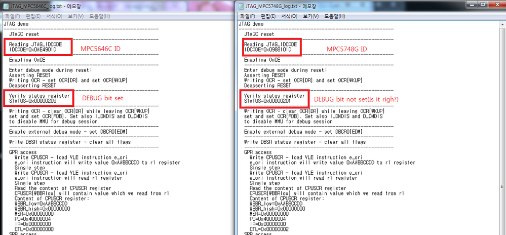
MPC5646C is entered debug mode but MPC5748G is not entered debug mode.
ssd c55 flash driver load to sram and set PC and go.
but it is not go.
plz help how to go+exit ?
Original Attachment has been moved to: JTAG_MPC5646C.cmm.zip
Original Attachment has been moved to: JTAG_MPC5748G.cmm.zip
Solved! Go to Solution.
- Mark as New
- Bookmark
- Subscribe
- Mute
- Subscribe to RSS Feed
- Permalink
- Report Inappropriate Content
Hi,
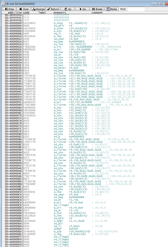
there's se_illegal instruction (0x0000) between two nop instructions (ori r0,r0,0x0). If this instruction is executed in external debug mode then debug mode is entered.
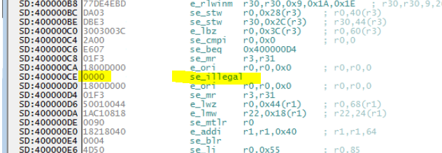
I tested it and it works as expected. It is necessary to set BDMEnabled to TRUE and then this code is executed at the end of function.
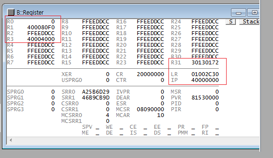
My question is: how did you set r1, r3 and ssd_config structure before executing the function?
Regards,
Lukas
- Mark as New
- Bookmark
- Subscribe
- Mute
- Subscribe to RSS Feed
- Permalink
- Report Inappropriate Content
Hi,
The original cmm worked for me with old versions of the Calypso (1N81M), but it does not with the latest version (0N78S). Same symptom, debug mode not entered. Note the different JTAG ID for the new MCU.
Any ideas how to enter debug mode on this device?
JTAG demo
--------------------------------------------------------
JTAGC reset
------------------------------------------------------
Reading JTAG_IDCODE
IDCODE=0x0988201D
------------------------------------------------------
Enabling OnCE
------------------------------------------------------
Enter debug mode during reset:
Asserting RESET
Writing OCR - set OCR[DR] and set OCR[WKUP]
Deasserting RESET
Verify status register
STATUS=0x00000201
------------------------------------------------------
Disable watchdog
Data=0x0A0100FF
------------------------------------------------------
Verify status register
STATUS=0x00000201
- Mark as New
- Bookmark
- Subscribe
- Mute
- Subscribe to RSS Feed
- Permalink
- Report Inappropriate Content
Oops it works, but somehow slower than Cut 2.0. The 100ms delay is really needed. 1N81M worked with 50us.
- Mark as New
- Bookmark
- Subscribe
- Mute
- Subscribe to RSS Feed
- Permalink
- Report Inappropriate Content
- Mark as New
- Bookmark
- Subscribe
- Mute
- Subscribe to RSS Feed
- Permalink
- Report Inappropriate Content
FlashInit VLE Assem code under
Where is BDM Enable code on C55 SRecord Firmware VLE Assem?
- Mark as New
- Bookmark
- Subscribe
- Mute
- Subscribe to RSS Feed
- Permalink
- Report Inappropriate Content
Hi,
there's se_illegal instruction (0x0000) between two nop instructions (ori r0,r0,0x0). If this instruction is executed in external debug mode then debug mode is entered.

I tested it and it works as expected. It is necessary to set BDMEnabled to TRUE and then this code is executed at the end of function.
My question is: how did you set r1, r3 and ssd_config structure before executing the function?
Regards,
Lukas
- Mark as New
- Bookmark
- Subscribe
- Mute
- Subscribe to RSS Feed
- Permalink
- Report Inappropriate Content
my gpio jtag initialize sequence below.
i think go +exit function is incorrect. ??
or interrupt blocked ?
Could you give me go+exit script to run on T32?
// 1. Assert RESET
sleep_ms(10);
// 2. Set the OCMD_ENABLE_ONCE[0xFFFFFFFF]
// 3. Set the OCR[DR] and OCR[WKUP]
// 4. Deassert RESET
sleep_ms(10);
// 5. Verify debug mode via the DEBUG bit in the OnCE status register
//6. External Debug Mode Enable
once_reg_write(bus, "OCMD_EDBCR0", DBCR0_EDM); // set EDBCR0[EDM]
once_reg_write(bus, "OCMD_DBCR0", DBCR0_EDM); // set EDBCR0[EDM]
once_reg_write(bus, "OCMD_DBSR", 0xFFFFFFFF); // clear DBSR
//7. Sram Init
//8. FMPLL init
//9. Load C55 S-Record file(i think file crc error. (???))
//10. c55_config write to sram
// 11.c55_FlashInit()
//11.1 write PC
/* no-op = e_ori 0,0,0 */
cpuscr_data.ir = 0x1800D000;
cpuscr_data.pc = data - 4;
cpuscr_data.ctl = (CPUSCR_CTL_WAITING | CPUSCR_CTL_IRSTAT8);
once_single_step(bus, cpuscr_data);
//11.2 go~~~
once_reg_write(bus, "OCMD_OCR", (OCR_WKUP | OCR_FDB));
once_ir_exec(bus, "OCMD_OSR", OCMD_READ, OCMD_GO, OCMD_LEAVE_DBG);
// 11.3 wait for Debug bit set
OCMD_NOREGSELECT read but not set debug bit so time out!!!
- Mark as New
- Bookmark
- Subscribe
- Mute
- Subscribe to RSS Feed
- Permalink
- Report Inappropriate Content
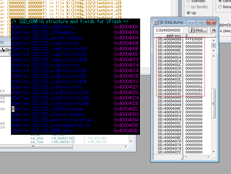
My ssd_config information and r1,r3 value is under picture.
is it right?
c55RegBase = 0xFFFE0000;
mainArrayBase = 0x00404000;
lowBlockInfo.n16KBlockNum = 0;
lowBlockInfo.n32KBlockNum = 0;
lowBlockInfo.n64KBlockNum = 0;
midBlockInfo.n16KBlockNum = 0;
midBlockInfo.n32KBlockNum = 0;
midBlockInfo.n64KBlockNum = 0;
highBlockInfo.n16KBlockNum = 0;
highBlockInfo.n32KBlockNum = 0;
highBlockInfo.n64KBlockNum = 0;
n256KBlockNum = 0;
uTestArrayBase = 0x00400000;
mainInterfaceFlag = 0x1;
programmableSize = 0x80;
BDMEnable = 0x01;
- Mark as New
- Bookmark
- Subscribe
- Mute
- Subscribe to RSS Feed
- Permalink
- Report Inappropriate Content
Hi,
I tested it using this config structure:

The BOOL is defined as "typedef unsigned char BOOL;" in ssd_types.h, so the alignment is different. Could you give this a try?
Regards,
Lukas
- Mark as New
- Bookmark
- Subscribe
- Mute
- Subscribe to RSS Feed
- Permalink
- Report Inappropriate Content
Thank you for your reply.
I am very happy. I can go to next step.
I suffered for 3 week.
Thank you.
- Mark as New
- Bookmark
- Subscribe
- Mute
- Subscribe to RSS Feed
- Permalink
- Report Inappropriate Content
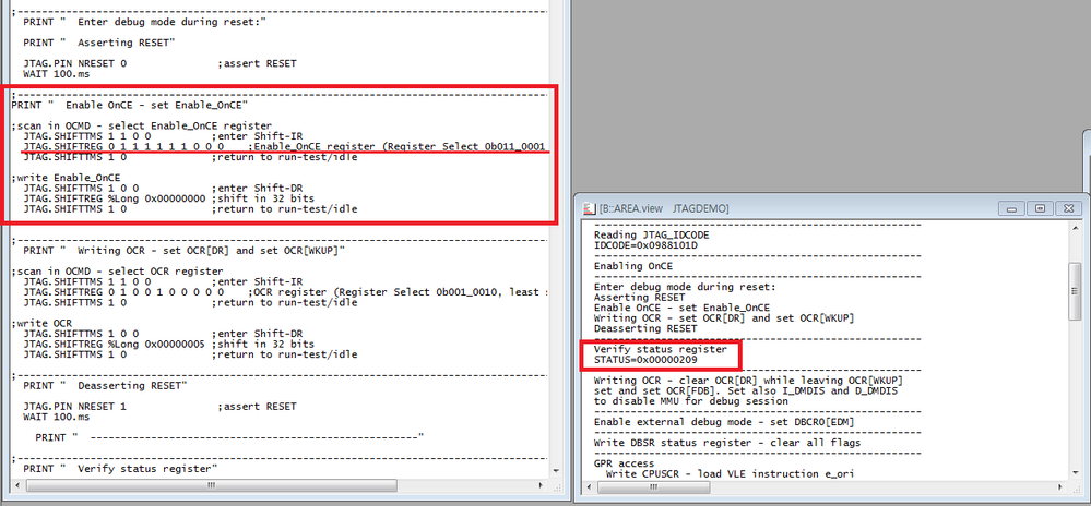
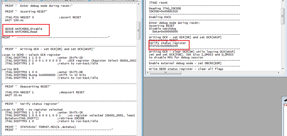
Thank you for your reply.
I tested for 2 things. i can entered debug mode.
1. Write OnCE Command : 111 1110 Enable_OnCE
1. Refer to MPC5748G Refernce Manual Rev 4, 07/2015
2. Page 3146 section 62.8 Basic Steps for Enableing, Using, and Exiting External Debug Mode
2. watchdog disable(my c code tested, your script modify)
1. Assert Reset
2. disable watchdog
3. set OCR[DR | WKUP]
4. Deassert Reset
I have last problem.
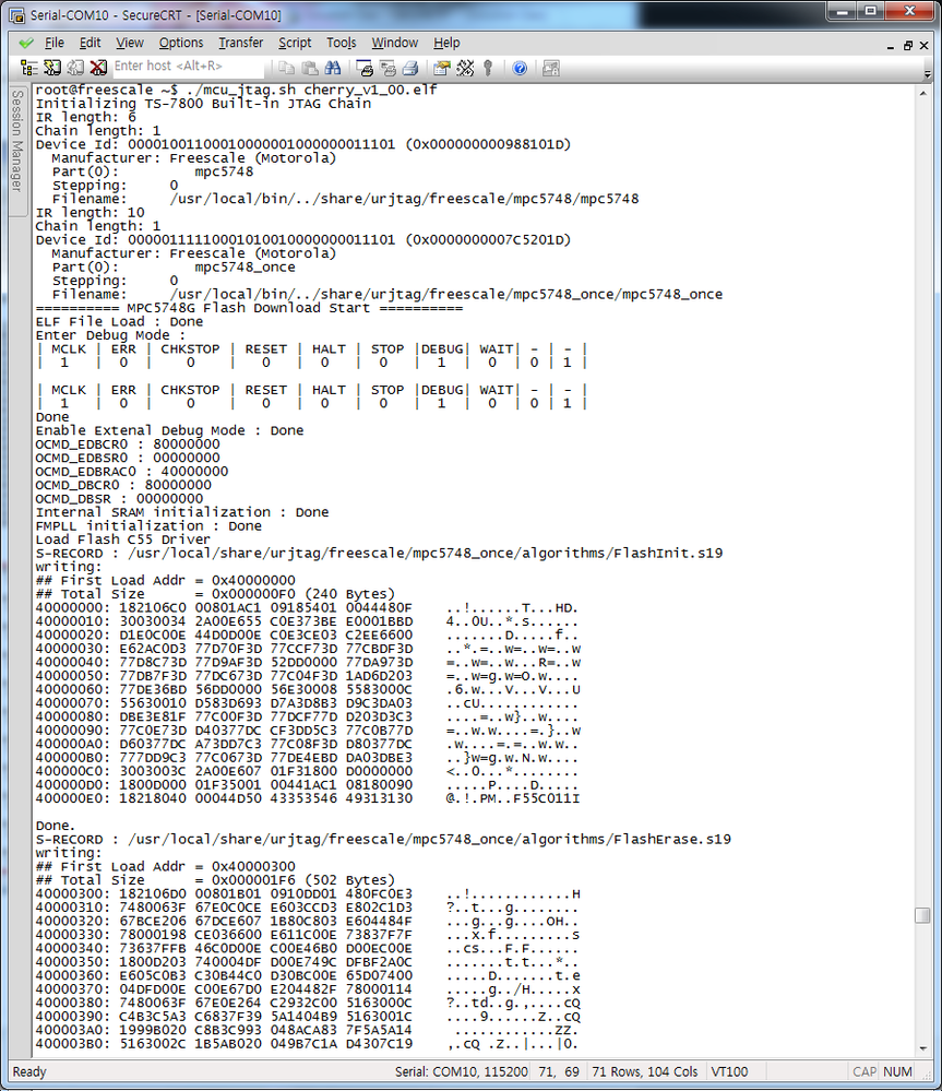
I loaded at sram c55 flash firmware driver.
I checked ok form T32 memory dump.
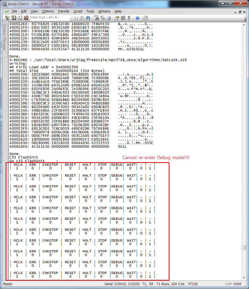
I wrote CPUSCR (PC 0x40000000 - 4, "no reg sel", Go + Exit) for run FlashInit function.
That is not re-entered debug mode.
searching data sheet....... now....(EDBCR0, Access to Debug Resources, ... i don`t know how to control other register.)
MPC5646C working is good but MPC5748G working is not good. so a little different how to control.
