- NXP Forums
- Product Forums
- General Purpose MicrocontrollersGeneral Purpose Microcontrollers
- i.MX Forumsi.MX Forums
- QorIQ Processing PlatformsQorIQ Processing Platforms
- Identification and SecurityIdentification and Security
- Power ManagementPower Management
- MCX Microcontrollers
- S32G
- S32K
- S32V
- MPC5xxx
- Other NXP Products
- Wireless Connectivity
- S12 / MagniV Microcontrollers
- Powertrain and Electrification Analog Drivers
- Sensors
- Vybrid Processors
- Digital Signal Controllers
- 8-bit Microcontrollers
- ColdFire/68K Microcontrollers and Processors
- PowerQUICC Processors
- OSBDM and TBDML
-
- Solution Forums
- Software Forums
- MCUXpresso Software and ToolsMCUXpresso Software and Tools
- CodeWarriorCodeWarrior
- MQX Software SolutionsMQX Software Solutions
- Model-Based Design Toolbox (MBDT)Model-Based Design Toolbox (MBDT)
- FreeMASTER
- eIQ Machine Learning Software
- Embedded Software and Tools Clinic
- S32 SDK
- S32 Design Studio
- Vigiles
- GUI Guider
- Zephyr Project
- Voice Technology
- Application Software Packs
- Secure Provisioning SDK (SPSDK)
- Processor Expert Software
-
- Topics
- Mobile Robotics - Drones and RoversMobile Robotics - Drones and Rovers
- NXP Training ContentNXP Training Content
- University ProgramsUniversity Programs
- Rapid IoT
- NXP Designs
- SafeAssure-Community
- OSS Security & Maintenance
- Using Our Community
-
-
- Home
- :
- Product Forums
- :
- S12 / MagniV Microcontrollers
- :
- we have a problem in using mc9s12hy64 during developping a board, that is our board will reset when using a cellphone to call out,that maybe EMC problem
we have a problem in using mc9s12hy64 during developping a board, that is our board will reset when using a cellphone to call out,that maybe EMC problem
- Subscribe to RSS Feed
- Mark Topic as New
- Mark Topic as Read
- Float this Topic for Current User
- Bookmark
- Subscribe
- Mute
- Printer Friendly Page
we have a problem in using mc9s12hy64 during developping a board, that is our board will reset when using a cellphone to call out,that maybe EMC problem
- Mark as New
- Bookmark
- Subscribe
- Mute
- Subscribe to RSS Feed
- Permalink
- Report Inappropriate Content
When we put a cellphone close to our board ,it is likely that the mcu will reset, but not all the phone can cause this problem, and only when the phone is in calling someone and his phone doesn't have alarm;
our board using mc9s12hy64 mcu, using outside 8m frequency crystal oscillator, an the software config the mcu using a frequency of 64M ,so the bus clock is 32M , the software config init code as below:
{
unsigned char i = 255;
CPMUPROT = 0x26;
CPMUCLKS_PLLSEL = 1;
CPMUREFDIV = 0x80; /* Config fREF 4M */
CPMUSYNR = 0x43; /* Config fVCO 64M */
CPMUPOSTDIV = 0x00; /* Config fPLL 64M fBus 32M */
CPMUOSC_OSCE = 1; /* enable ext OSC */
do{
i--;
}while((!CPMUFLG_UPOSC || !CPMUFLG_LOCK) && (i));
/* wait for ext osc to stabilize and pll to lock */
CPMUFLG = 0xFF;
CPMUCLKS = 0x81; /* RTI COP clock source is oscclk */
CPMUCOP = 0x46;
/* watchdog reset time 1.04S */
CPMURTI = 0xF9; /* RTI Time 0.25s */
CPMUINT_RTIE = 0; /* enable RTI interrupt */
while( CPMUCLKS != 0x81 )
{
CPMUCLKS = 0x81;
}
CPMUPROT = 0x01; /* Protect pll clock */
}
Can anyone give an advise or give me some direction?
- Mark as New
- Bookmark
- Subscribe
- Mute
- Subscribe to RSS Feed
- Permalink
- Report Inappropriate Content
Hi,
it is not clear whether you are talking about your own design or standard evaluation board. However, the isues you describe leads me to your own design. The clocks look to be set correctly. Have you tried to use lower BUSCLK whether there is still the same problem?
If I were you I would check following:
1) Correct load capacitance connected to a crystal. simplified C1=C2 >= 2*Cload (internal capacitance of the pins is omitted)
Moreover I would like to give you some recommendations:
- Crystals with fundamental frequency are recommended.
- Use crystals with low drive level.
- I believe you use standard and recommended PCB layout for oscillator circuitry.
- The crystal with good DC bias immunity should be used
- Cdc impedance value should be smallest – less than 1kohm. (Cdc = 10nF is good for oscillator for 32kHz and above).
2) Schematic design review.
3) PCB design of oscillator circuitry review, There are not allowed any logic or analog or ground wires or planes under oscillator circuitry. It is recommended to use recommended PCB layout presented in the datasheet. the oscillator should use 1st harmonics.
If it is possible I would like to see schematic design in the first approach. If it is confidential we can talk via another channel. You can create a service request ... described How to submit a new question for NXP Support
best regards,
Ladislav
- Mark as New
- Bookmark
- Subscribe
- Mute
- Subscribe to RSS Feed
- Permalink
- Report Inappropriate Content
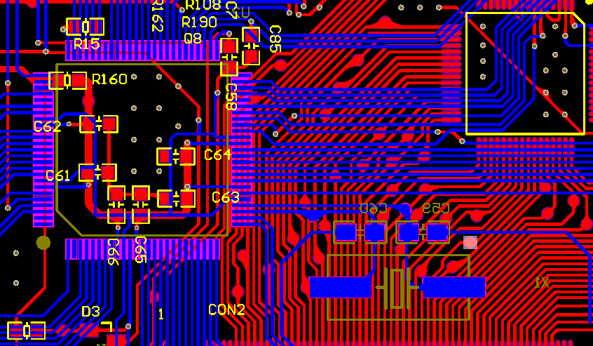
"There are not allowed any logic or analog or ground wires or planes under oscillator circuitry" Does the other side of the oscillator included? Our board had a lot of wire on the other side of the oscillator, this wire is mainly for lcd driver use, but when I write a software that don't use the lcd driver chip , the problem continue to happen.
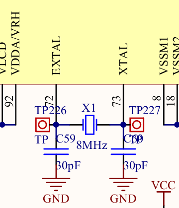
oscillator circuitry is as bellow
- Mark as New
- Bookmark
- Subscribe
- Mute
- Subscribe to RSS Feed
- Permalink
- Report Inappropriate Content
Hi,
this is I was afraid of.
I would like to show you Oscillator Layout Considerations from AN3262 (Designing Hardware for the 9S12XD family) which is for different MCU but principle is the same. (http://www.nxp.com/assets/documents/data/en/application-notes/AN3262.pdf )
9.1 Oscillator Layout Considerations
Good practice is important when laying out a PCB for any oscillator configuration and it is a good idea to
lay out the oscillator first in any design.
The PCB layout is equally as critical when using a ceramic resonator as when using a quartz crystal
resonator.
Keep the oscillator components on the same side of the PCB as the MCU and as close to the MCU as
possible (allowing for the fan-out of any I/O used on the oscillator side of the MCU).
Parasitic capacitance between EXTAL and XTAL must be kept to a minimum. The EXTAL and XTAL
tracks should be kept short and routed apart.
Take care when mounting a metal cased resonator directly on a PCB where the case of the oscillator will
be in close proximity to the EXTAL and XTAL tracks on the board, as the case can introduce parasitic
capacitance between the two signals. Where this might occur, consider mounting the resonator on its side,
introducing some spacing between the resonator case and the PCB, or grounding the oscillator case.
A ground plane under the oscillator circuit is not a concern and can be advantageous as it can prevent
signals on adjacent layer interfering with the oscillator (any increased parasitic loading from EXTAL and
XTAL tracks to the ground plane can be evaluated and could be compensated for in the load capacitor
values).
Where possible, keep the oscillator tracks on the same side of the PCB as the oscillator — minimize vias
in the oscillator circuit.
Where there is no ground plane under the oscillator, avoid routing other signals on any layers in the region
of the oscillator components or tracks. Place an exclusion zone on all layers around the oscillator.
Include a decoupling capacitor close to the VDDPLL/VSSPLL pins. Avoid vias in the VxxPLL supply tracks
from the decoupling capacitor.
Treat the ground signal for the oscillator as a separate ground, connecting to the main digital ground at one
point only, close by VSSR. Where the main digital ground is implemented with a ground plane, it is
recommended to keep the oscillator / PLL ground separate from the ground plane. Avoid connecting
external components connected to digital IO (pull devices, filter circuits, for example) to the oscillator
ground to prevent noise or transitions on the IO signals disturbing the oscillator.
Routing the oscillator ground via the TEST pin can simplify the layout. (The TEST pin is a static digital
input that will not disturb the oscillator ground.)
Keep the adjacent RESET signal clean. Where it is connected off the board or to a long track in a noisy
environment, consider adding some series resistance.
Avoid routing signals under the PLL components or tracks, to minimize cross-talk.
These guidelines are valid for single sided, double sided, and multi-layer boards. On boards with multiple
layers, it may be possible to locate the oscillator closer to the MCU by fanning out the adjacent I/O
underneath the MCU. Moving the PLL filter components to the underside of the board will also help
simplify the tracking adjacent to the oscillator.
You have now two ways of solution. Either redesign PCB or use internal oscillator.
Best regards,
Ladislav
- Mark as New
- Bookmark
- Subscribe
- Mute
- Subscribe to RSS Feed
- Permalink
- Report Inappropriate Content
Thank you, these day we did a lot of jobs , and we dug the board and the circuit on the board almost only mcu and oscillator and the copper foil on both side almost none, and still problems exsit, Now we redesigned our pcb, and the pcb is not returned ,we want to find where influence it;
We did a test two days ago, and our board can endure 140v/m at 820MHZ ~ 900MHZ, but failed at 200V/m the same frequency, and we will test our cellphone capacity to find if it is in this stage.

