- NXP Forums
- Product Forums
- General Purpose MicrocontrollersGeneral Purpose Microcontrollers
- i.MX Forumsi.MX Forums
- QorIQ Processing PlatformsQorIQ Processing Platforms
- Identification and SecurityIdentification and Security
- Power ManagementPower Management
- MCX Microcontrollers
- S32G
- S32K
- S32V
- MPC5xxx
- Other NXP Products
- Wireless Connectivity
- S12 / MagniV Microcontrollers
- Powertrain and Electrification Analog Drivers
- Sensors
- Vybrid Processors
- Digital Signal Controllers
- 8-bit Microcontrollers
- ColdFire/68K Microcontrollers and Processors
- PowerQUICC Processors
- OSBDM and TBDML
-
- Solution Forums
- Software Forums
- MCUXpresso Software and ToolsMCUXpresso Software and Tools
- CodeWarriorCodeWarrior
- MQX Software SolutionsMQX Software Solutions
- Model-Based Design Toolbox (MBDT)Model-Based Design Toolbox (MBDT)
- FreeMASTER
- eIQ Machine Learning Software
- Embedded Software and Tools Clinic
- S32 SDK
- S32 Design Studio
- Vigiles
- GUI Guider
- Zephyr Project
- Voice Technology
- Application Software Packs
- Secure Provisioning SDK (SPSDK)
- Processor Expert Software
-
- Topics
- Mobile Robotics - Drones and RoversMobile Robotics - Drones and Rovers
- NXP Training ContentNXP Training Content
- University ProgramsUniversity Programs
- Rapid IoT
- NXP Designs
- SafeAssure-Community
- OSS Security & Maintenance
- Using Our Community
-
-
- Home
- :
- General Purpose Microcontrollers
- :
- Kinetis Microcontrollers
- :
- Kinetis K64F missing documentation?
Kinetis K64F missing documentation?
- Subscribe to RSS Feed
- Mark Topic as New
- Mark Topic as Read
- Float this Topic for Current User
- Bookmark
- Subscribe
- Mute
- Printer Friendly Page
Kinetis K64F missing documentation?
- Mark as New
- Bookmark
- Subscribe
- Mute
- Subscribe to RSS Feed
- Permalink
- Report Inappropriate Content
We're evaluating the K64F for a family of instrumentation products, but I'm having trouble finding all the required documentation. On the NXP web site, I find only two documents about this chip:
K64P144M120SF5RM.pdf: K64 Sub-Family Reference Manual, Rev. 2, January 2014
K64P144M120SF5.pdf: Kinetis K64F Sub-Family Data Sheet, Rev. 6, 08/2015
Questions:
- In the reference manual, in many places it says "Refer to chip configuration details".
Where are "chip configuration details"? - Reference manual page 934, PDBx_SC field descriptions, Trigger Input Source Select, says:
"Refer to chip configuration details for the actual PDB input trigger connections."
Where is the table defining the values and possible PDB input triggers? - Reference manual page 459, DMAMUX_CHCFGn field descriptions DMA Channel Source, says:
"See your device's chip configuration details for information about the peripherals and their slot numbers."
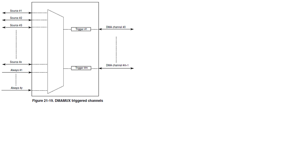
Where is the table defining allowed values and corresponding peripherals? - Reference manual section 21.5.2, To enable a source with periodic triggering, step 5 says:
"Select the source to be routed to the DMA channel. Write to the corresponding
CHCFG register" - This appears to be an error.
For periodic triggering, the source must be set to an "always on" source, right? - Where is the table of application notes, with links to the notes and associated source code, for Kinetis processors?
The last thing I find with google is a list without links last updated in 2012...
Without this information, it is very hard for your customers to make use of these parts...
Any help would be much appreciated.
Thanks!
Best Regards, Dave
- Mark as New
- Bookmark
- Subscribe
- Mute
- Subscribe to RSS Feed
- Permalink
- Report Inappropriate Content
Hi,
Pls refer to chapter 3 chip configuration in K64P144M120SF5RM.pdf.
For PDB triggering source, pls refer to section 3.8.1.1.2 PDB Input Trigger Connections.
For DMA requestion source, pls refer to section 3.3.9.1 DMA MUX request sources
Hope it can help you
BR
XiangJun Rong
- Mark as New
- Bookmark
- Subscribe
- Mute
- Subscribe to RSS Feed
- Permalink
- Report Inappropriate Content
Hello XiangJun Rong - We are still waiting for answers to 4,5, and 6 above? It has been almost one month?
Answers would be much appreciated!
Thanks, Best Regards, Dave
- Mark as New
- Bookmark
- Subscribe
- Mute
- Subscribe to RSS Feed
- Permalink
- Report Inappropriate Content
Hi, Dave,
I am sorry for the delay. Regarding the GPIO toggling based on DMA plus PIT, You have to use DMA channel0 if you use PIT0 to trigger, use DMA channel1 if you use PIT1. I attach the fig here.
For DGPIO configuration, you have to set the PORTx_PCRy as GPIO function and set the IRQC bits as 3(DMA request on either edge.). For example, if you use PIT0, you have to use DMA channel0. Set the source bits of DMAMUX_CHCFG0 as 49(PORTA), 50(PORTB), 51 (PORTC)..., configure PIT0 registers and DMA registers, it is okay.
BR
Xiangjun rong
- Mark as New
- Bookmark
- Subscribe
- Mute
- Subscribe to RSS Feed
- Permalink
- Report Inappropriate Content
- Mark as New
- Bookmark
- Subscribe
- Mute
- Subscribe to RSS Feed
- Permalink
- Report Inappropriate Content
Thanks! To save other customers trouble, please consider updating the manual adding links in the PDF to the mentioned chapter, or at a very minimum say "Refer to chip configuration details chapter above"... I was looking for a separate document (as have other customers asking this question on this forum).
Can you answer questions 4 and 5 above?
Also, another apparent documentation error:
6) In reference manual 21.4.1 DMA channels with periodic triggering capability: PIT 1 is shown connected to DMA trigger 0. In reality, PIT 0 is connected to DMA trigger 0, right? Here's the erroneous diagram (also repeated in the text)
Thanks,
Best Regards, Dave

