- NXP Forums
- Product Forums
- General Purpose MicrocontrollersGeneral Purpose Microcontrollers
- i.MX Forumsi.MX Forums
- QorIQ Processing PlatformsQorIQ Processing Platforms
- Identification and SecurityIdentification and Security
- Power ManagementPower Management
- MCX Microcontrollers
- S32G
- S32K
- S32V
- MPC5xxx
- Other NXP Products
- Wireless Connectivity
- S12 / MagniV Microcontrollers
- Powertrain and Electrification Analog Drivers
- Sensors
- Vybrid Processors
- Digital Signal Controllers
- 8-bit Microcontrollers
- ColdFire/68K Microcontrollers and Processors
- PowerQUICC Processors
- OSBDM and TBDML
-
- Solution Forums
- Software Forums
- MCUXpresso Software and ToolsMCUXpresso Software and Tools
- CodeWarriorCodeWarrior
- MQX Software SolutionsMQX Software Solutions
- Model-Based Design Toolbox (MBDT)Model-Based Design Toolbox (MBDT)
- FreeMASTER
- eIQ Machine Learning Software
- Embedded Software and Tools Clinic
- S32 SDK
- S32 Design Studio
- Vigiles
- GUI Guider
- Zephyr Project
- Voice Technology
- Application Software Packs
- Secure Provisioning SDK (SPSDK)
- Processor Expert Software
-
- Topics
- Mobile Robotics - Drones and RoversMobile Robotics - Drones and Rovers
- NXP Training ContentNXP Training Content
- University ProgramsUniversity Programs
- Rapid IoT
- NXP Designs
- SafeAssure-Community
- OSS Security & Maintenance
- Using Our Community
-
- Cloud Lab Forums
-
- Home
- :
- General Purpose Microcontrollers
- :
- LPC Microcontrollers
- :
- LPC4370 SSP SPI 8bit problem
LPC4370 SSP SPI 8bit problem
- Subscribe to RSS Feed
- Mark Topic as New
- Mark Topic as Read
- Float this Topic for Current User
- Bookmark
- Subscribe
- Mute
- Printer Friendly Page
- Mark as New
- Bookmark
- Subscribe
- Mute
- Subscribe to RSS Feed
- Permalink
- Report Inappropriate Content
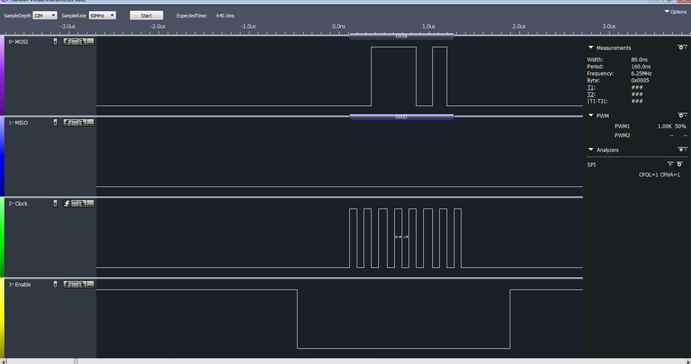
I am implementing SPI on LPC4370 SSP. I have configured for 8-bit frame.
However when I write to the DR register it outputs 16 bits, the first byte seems to be what was entered 8 frames ago and the second byte is what I just entered.
Is this a known problem with a workaround?
or is something configured wrong?
CCR0 = 0x07,
CCR1= 0x02
Original Attachment has been moved to: SSP_SPI_Test.zip
Solved! Go to Solution.
- Mark as New
- Bookmark
- Subscribe
- Mute
- Subscribe to RSS Feed
- Permalink
- Report Inappropriate Content
Hi Raymundo Velarde,
After a lot of test on my side, I found it may relate to the clock in your project, the desynchrony between the SSP register clock and the peripheral clock.
You configure BASE_M4_CLK =2Mhz, source is IDVC/6 from crystal 12Mhz.
BASE_SSP1_CLK = 12Mhz, source is from crystal 12Mhz directly.
Now, I am not sure whether the LPC43XX need the peripheral clock should not larger than register clock, but from my test, if the peripheral clock is not larger than register clock, your problem will be solved in your code, and the data also have no lag.
My modifications conclusion:
Also configure BASE_SSP1_CLK =2Mhz, source is IDVC/6 from crystal 12Mhz, then the ssp baud rate configure as 1Mhz, because the SSP clock must be divided 2 in master mode.
Now, my test result is correct, no matter clock ssp frequent, or the ssp data.
Could you please test my way on your side?
Just a small modification on your project, main.c
int main(void)
{
//===========================================jjadd b
int i = 0;
uint8_t data[] = {0x11, 0x22, 0x33, 0x44, 0x55, 0x66, 0x77, 0x88,
0x99, 0xAA, 0xBB, 0xCC, 0xDD, 0xEE, 0xFF, 0x0F};
Chip_Clock_SetBaseClock(CLK_BASE_SSP1, CLKIN_IDIVC, true, false); //jjadd BASE_SSP1_CLK from IDIVC 2Mhz
SystemCoreClockUpdate();
Board_Init();
...
}
Just add the red line in the above, then test it again on your side.
My test result is:
Actually, I also try other clock source, just make sure the peripheral clock is not larger than register clock, the data is correct, and have no lag.
About the detail reason of this question, I will also check it with our AE department, If I get the reasonable feedback, I will let your know!
Have a great day,
Kerry
-----------------------------------------------------------------------------------------------------------------------
Note: If this post answers your question, please click the Correct Answer button. Thank you!
-----------------------------------------------------------------------------------------------------------------------
- Mark as New
- Bookmark
- Subscribe
- Mute
- Subscribe to RSS Feed
- Permalink
- Report Inappropriate Content
Kerry, thank you, it works.
I tested several settings and it seems that the output of the SSP prescaler has to be a value that corresponds to the SSP Register Clock divided by an even number(Possible CPSR value).
For example I did not change my clock settings (MCU + SSP Register Clock = 2MHz, and SSP peripheral clock = 12MHz), but used CPSR = 12 (output 1MHz achievable by 2MHz/2), CPSR = 24 (Output 500KHz achievable by 2MHz/4) and CPSR = 36 (Output 3331/3KHz achievable by 2MHz/6) and they all work.
However CPSR = 16 (750KHz not achievable by 2MHz with any CPSR setting) does not work.
So apparently, the only way to guarantee that the settings work is to have the SSP peripheral clock be the same as the SSP registers clock. It is probably related to the fact that the data is set through the DR register running at the register clock rate. This defeats the advantage of being able to specify different peripheral and register clocks.
We were trying to have the CPU use less power by running slow but control some hardware qickly with spi by running the ssp peripheral at 6MHz, but it is impossible. At least now we understand what is going on.
- Mark as New
- Bookmark
- Subscribe
- Mute
- Subscribe to RSS Feed
- Permalink
- Report Inappropriate Content
Hi Raymundo,
Could you post more code about your SSP operation?
It seems you send two 8 bits data, not just send one 16 bit data.
Please give me your SSP code in your main function.
Waiting for your reply!
Have a great day,
Kerry
-----------------------------------------------------------------------------------------------------------------------
Note: If this post answers your question, please click the Correct Answer button. Thank you!
-----------------------------------------------------------------------------------------------------------------------
- Mark as New
- Bookmark
- Subscribe
- Mute
- Subscribe to RSS Feed
- Permalink
- Report Inappropriate Content
Here is my initialization code.
void SPI_Init(LPC_SSP_T *pSSP, uint32_t bitRate)
{
CHIP_CCU_CLK_T CLK_MX_SSPx = (pSSP == LPC_SSP0)?CLK_MX_SSP0:CLK_MX_SSP1;
Chip_SSP_Disable(pSSP);
Chip_Clock_Enable(CLK_MX_SSPx);
Chip_SSP_Set_Mode(pSSP, SSP_MODE_MASTER);
/* todo: Format fixed for now. Do we need flexibility to change it for Comm board? */
Chip_SSP_SetFormat(pSSP, SSP_BITS_8, SSP_FRAMEFORMAT_SPI, SSP_CLOCK_MODE0);
Chip_SSP_SetBitRate(pSSP, bitRate);
Chip_SSP_Enable(pSSP);
}
I am writing a spi flash driver. One of the first things I have to do before writing is send a write enable command. Here is the code.
IO_SetPinState(SPI_CSPort, SPI_CSPin, false);
delayUS(1);
Chip_SSP_SendFrame(LPC_SSP1, WRITE_ENABLE);
while (Chip_SSP_GetStatus(LPC_SSP1, SSP_STAT_BSY) == SET);
IO_SetPinState(SPI_CSPort[1], SPI_CSPin[1], true);
Since the driver was not working, I set a breakpoint after this. I noticed that two bytes were output.
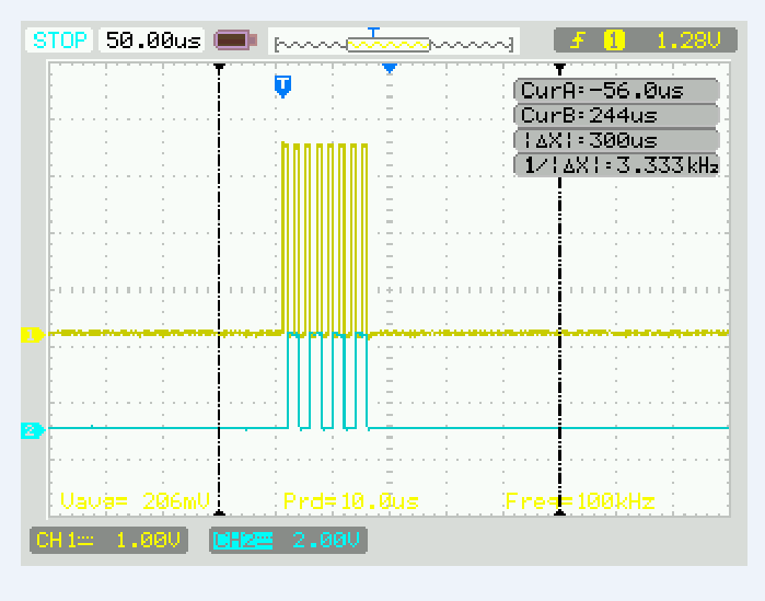
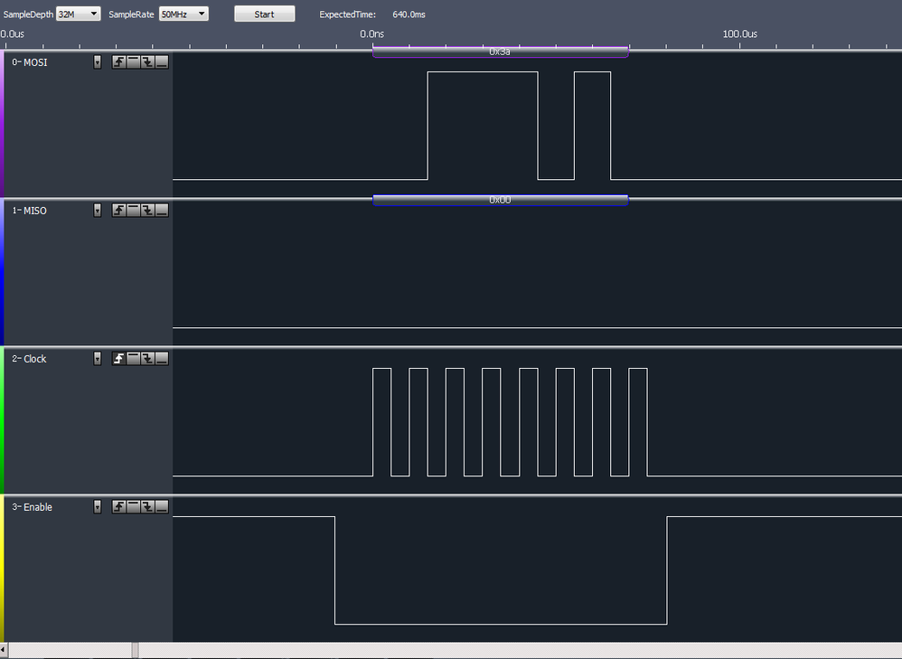
The waveform I previously attached was generated with the program stopped at the breakpoint and just writing 0x3A to the SSP1->DR register, so I am sure no other byte was written.
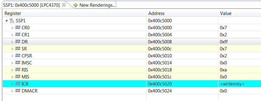
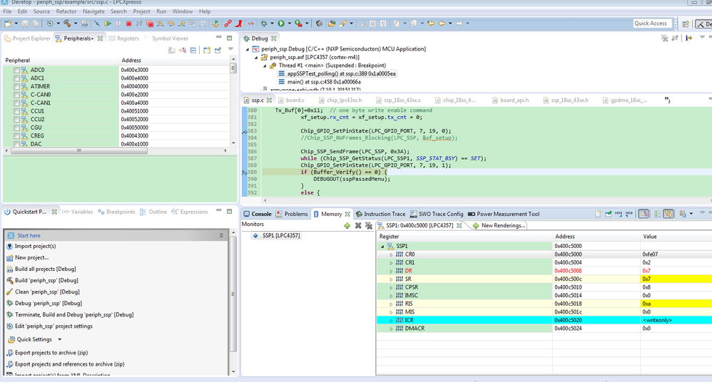
These are the Register settings.
- Mark as New
- Bookmark
- Subscribe
- Mute
- Subscribe to RSS Feed
- Permalink
- Report Inappropriate Content
Hi Raymundo,
Please refer to our LPCopen ssp sample code, it also configure the data as 8bit.
I have test this code, it works ok on my side, when I just send one byte data, you can download the code from this link:
Find the SSP code in folder:lpcopen_2_12_lpcxpresso_nxp_lpclink2_4370\periph_ssp
I modify these points:
1. #define BUFFER_SIZE (0x1)
2. add Tx_Buf[0] =0X55; in static void appSSPTest(void) like this:
static void appSSPTest(void)
{
int key;
DEBUGOUT(sspTransferModeSel);
dmaChSSPTx = Chip_GPDMA_GetFreeChannel(LPC_GPDMA, LPC_GPDMA_SSP_TX);
dmaChSSPRx = Chip_GPDMA_GetFreeChannel(LPC_GPDMA, LPC_GPDMA_SSP_RX);
xf_setup.length = BUFFER_SIZE;
xf_setup.tx_data = Tx_Buf;
xf_setup.rx_data = Rx_Buf;
while (1) {
key = 0xFF;
do {
key = DEBUGIN();
} while ((key & 0xFF) == 0xFF);
Buffer_Init();
Tx_Buf[0] =0X55;
After testing , the result is like the following picture, it only sends one byte.
so, please refer to the lpcopen sample code, check your own configuration and calling again.
Wish it helps you!
If you still have question, please let me know!
Have a great day,
Kerry
-----------------------------------------------------------------------------------------------------------------------
Note: If this post answers your question, please click the Correct Answer button. Thank you!
-----------------------------------------------------------------------------------------------------------------------
- Mark as New
- Bookmark
- Subscribe
- Mute
- Subscribe to RSS Feed
- Permalink
- Report Inappropriate Content
I forgot to add. I also need to control the SSEL by software because it needs to stay on for several bytes.
For example I need to:
SSEL on
send write enable (1 byte) command
SSEL off
SSEL on
send program command
send address (3 or 4 bytes)
send data (1 - 128 bytes)
SSEL off
- Mark as New
- Bookmark
- Subscribe
- Mute
- Subscribe to RSS Feed
- Permalink
- Report Inappropriate Content
Hi Raymundo,
Actually, my above reply is just based on the polling mode.
Now answer your question in details.
Because the SSEL will be controlled by the SSP module, then this pin will pull up after each byte sending.
Now, if you want to control the SSEL pin freely, you can configure this pin as the GPIO, then use the software to control it.
I have modify the SSP code which can realize your function, for simply showing, I modify your demand like this:
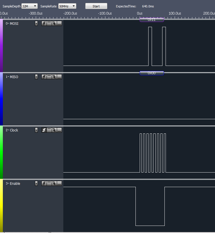
SSEL on
send write enable (1 byte 0x11) command
SSEL off
SSEL on
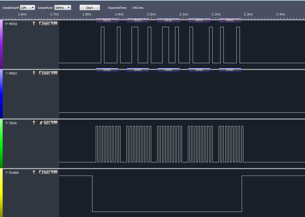
send program command(0x21)
send address (2bytes: 0x31,0x32)
send data (2bytes: 0x41,0x42)
SSEL off
If you want to have different bytes, just change the number.
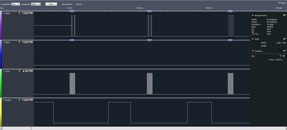
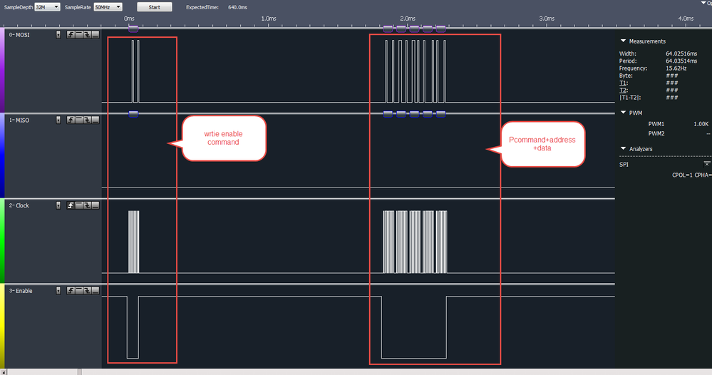
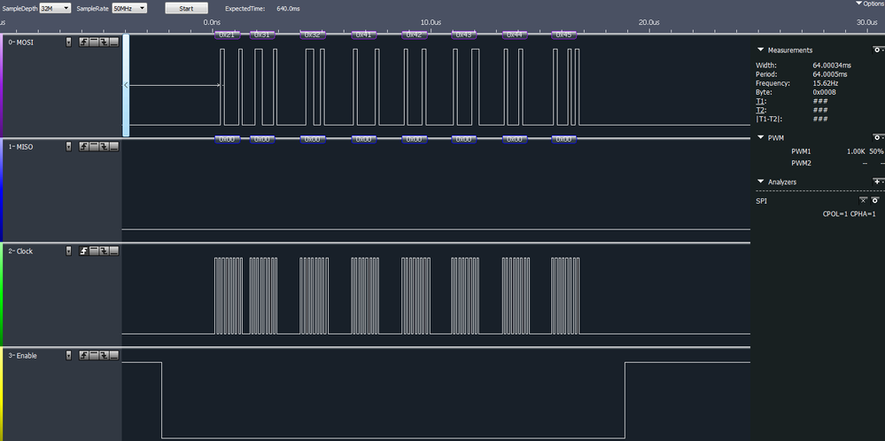
Then the test result wave from logic analyzer are like this:
zoom in:
Because I didn't add the SPI slave, the MISO don't have the data, but the Master polling control are sending the data which you want.
My polling function is like this:
static void appSSPTest_polling(void)
{
int key;
// dmaChSSPTx = Chip_GPDMA_GetFreeChannel(LPC_GPDMA, LPC_GPDMA_SSP_TX);
// dmaChSSPRx = Chip_GPDMA_GetFreeChannel(LPC_GPDMA, LPC_GPDMA_SSP_RX);
/******************Send polling 1 byte 0X11*********************************/
xf_setup.length = 1;
xf_setup.tx_data = Tx_Buf;
xf_setup.rx_data = Rx_Buf;
Tx_Buf[0]=0x11; // one byte write enable command
xf_setup.rx_cnt = xf_setup.tx_cnt = 0;
Chip_GPIO_SetPinState(LPC_GPIO_PORT, 7, 19, 0);
Chip_SSP_RWFrames_Blocking(LPC_SSP, &xf_setup);
Chip_GPIO_SetPinState(LPC_GPIO_PORT, 7, 19, 1);
if (Buffer_Verify() == 0) {
DEBUGOUT(sspPassedMenu);
}
else {
DEBUGOUT(sspFailedMenu);
}
/******************Send polling 1 byte 0X11*********************************/
xf_setup.length = 5;
xf_setup.tx_data = Tx_Buf;
xf_setup.rx_data = Rx_Buf;
Tx_Buf[0]=0x21; // one byte program command
Tx_Buf[1]=0x31;// two bytes address
Tx_Buf[2]=0x32;// two bytes address
Tx_Buf[3]=0x41; // two bytes data
Tx_Buf[4]=0x42;// two bytes data
xf_setup.rx_cnt = xf_setup.tx_cnt = 0;
Chip_GPIO_SetPinState(LPC_GPIO_PORT, 7, 19, 0);
Chip_SSP_RWFrames_Blocking(LPC_SSP, &xf_setup);
Chip_GPIO_SetPinState(LPC_GPIO_PORT, 7, 19, 1);
if (Buffer_Verify() == 0) {
DEBUGOUT(sspPassedMenu);
}
else {
DEBUGOUT(sspFailedMenu);
}
DEBUGOUT(sspTransferModeSel);
while (1) {
}
}Board_SSP_Init(LPC_SSP_T *pSSP) function which you can find it in the lpc_board project, it is modified like this:
void Board_SSP_Init(LPC_SSP_T *pSSP)
{
if (pSSP == LPC_SSP0) {
/* Set up clock and power for SSP0 module */
/* Configure SSP0 pins*/
Chip_SCU_PinMuxSet(0x3, 3, (SCU_PINIO_FAST | SCU_MODE_FUNC2)); /* P3.3 connected to SCL/SCLK SCU_MODE_FUNC2=SSP0 SCK0 */
Chip_SCU_PinMuxSet(0x3, 6, (SCU_PINIO_FAST | SCU_MODE_FUNC2)); /* P3.6 connected to nCS SCU_MODE_FUNC2=SSP0 SSEL0 */
Chip_SCU_PinMuxSet(0x3, 7, (SCU_MODE_INACT | SCU_MODE_INBUFF_EN | SCU_MODE_ZIF_DIS | SCU_MODE_FUNC2)); /* P3.7 connected to SO SCU_MODE_FUNC2=SSP0 MISO0 */
Chip_SCU_PinMuxSet(0x3, 8, (SCU_MODE_INACT | SCU_MODE_INBUFF_EN | SCU_MODE_ZIF_DIS | SCU_MODE_FUNC2)); /* P3.8 connected to nSI SCU_MODE_FUNC2=SSP0 MOSI0 */
}
else if (pSSP == LPC_SSP1) {
/* Set up clock and power for SSP1 module */
/* Configure SSP1 pins*/
Chip_SCU_PinMuxSet(0xF, 4, (SCU_PINIO_FAST | SCU_MODE_FUNC0)); /* PF.4 connected to SCL/SCLK SCU_MODE_FUNC0 = SSP1 SCK1 */
// Chip_SCU_PinMuxSet(0xF, 5, (SCU_PINIO_FAST | SCU_MODE_FUNC2)); /* PF.5 connected to nCS SCU_MODE_FUNC2 = SSP1 SSEL1 */
Chip_SCU_PinMuxSet(0xF, 5, (SCU_MODE_PULLUP| SCU_MODE_HIGHSPEEDSLEW_EN | SCU_MODE_INBUFF_EN | SCU_MODE_ZIF_DIS | SCU_MODE_FUNC4)); /* PF.5 connected to nCS SCU_MODE_FUNC2 = GPIO */
Chip_GPIO_SetPinDIROutput(LPC_GPIO_PORT, 7, 19);//PF_5 mux4 = GPIO7[19]
Chip_GPIO_SetPinState(LPC_GPIO_PORT, 7, 19, 1);
Chip_SCU_PinMuxSet(0xF, 6, (SCU_MODE_INACT | SCU_MODE_INBUFF_EN | SCU_MODE_ZIF_DIS | SCU_MODE_FUNC2)); /* PF.6 connected to SO SCU_MODE_FUNC2 = SSP1 MISO1 */
Chip_SCU_PinMuxSet(0xF, 7, (SCU_MODE_INACT | SCU_MODE_INBUFF_EN | SCU_MODE_ZIF_DIS | SCU_MODE_FUNC2)); /* PF.7 connected to nSI SCU_MODE_FUNC2 = SSP1 MOSI1 */
}
else {
return;
}
}For your reference, I also attached my LPCxpresso SSP project.
Wish it helps you!
If you still have question, please let me know!
Have a great day,
Kerry
-----------------------------------------------------------------------------------------------------------------------
Note: If this post answers your question, please click the Correct Answer button. Thank you!
-----------------------------------------------------------------------------------------------------------------------
- Mark as New
- Bookmark
- Subscribe
- Mute
- Subscribe to RSS Feed
- Permalink
- Report Inappropriate Content
I am not working on the LINK2 board, I am working on our board with the spi flash installed, so I ca't run the sample code as it is.
I am following the sample code for initialization. I initialize the same way as shown in the init code I posted, and have the registers set as posted on the screen shot above.
It still sends the two bytes when I call Chip_SSP_SendFrame() or when I poke one byte to DR register.
Do you see any problem with my initialization?
Can you post the SSP register settings you have when you get the above results?
- Mark as New
- Bookmark
- Subscribe
- Mute
- Subscribe to RSS Feed
- Permalink
- Report Inappropriate Content
HI Raymundo,
My configuration is the same as you, except the SSP clock divider, but this should not influence the SPI send bit.
Your configuration is already 8 bit.
This is my register result after 0X3a:
Could you please send me your whole project?
I will check your project on my side.
Have a great day,
Kerry
-----------------------------------------------------------------------------------------------------------------------
Note: If this post answers your question, please click the Correct Answer button. Thank you!
-----------------------------------------------------------------------------------------------------------------------
- Mark as New
- Bookmark
- Subscribe
- Mute
- Subscribe to RSS Feed
- Permalink
- Report Inappropriate Content
My configuration is the same as you, except the SSP clock divider, but this should not influence the SPI send bit.
I agree, it shouldn't but it does.
To reduce power consumption I am running with PLL disabled clock directly from crystal (12MHz)
So Pre-scaler is set to 2 (lowest value) and the SCR bits in the CR0 register are set to 0 (1 pre-scaler clock per bit) this should allow me to run at a 6MHz bit-rate.
With this configuration I have the problem as described. Once I change the SCR bits to anything other than 0 the problem disappears.
Now my problem is that the byte it outputs is the byte written 8 frames ago. So I have to write 8 frames before I assert the chip select (it outputs 0xFF for the first 8 frames, no matter what I write to the DR register) and then I have to write 8 "dummy" frames afterwards to output all the frames that I want to send.
In short, the data output lags by 8 frames.
- Mark as New
- Bookmark
- Subscribe
- Mute
- Subscribe to RSS Feed
- Permalink
- Report Inappropriate Content
Hi Raymundo,
Thank you for your more details.
1. Clock source factor.
I also tried the 12Mhz as the SSP1 clock source, and configure SCR =0, CPSR=2.
I still can get the correct data, the ssp baud rate is 6Mhz.
Did you check your ssp baud rate, whether it is 6Mhz? I can't get the data from your picture.
Please also check the register: CGU->BASE-SSP1-CLK,
This is my test result:
You can find my clk frequent is about 6Mhz, actually, I also use the oscilloscope test it, it is really 6Mhz, the logic analyzer have little allowable errors.
This is my configuration:
ssp_format.frameFormat = SSP_FRAMEFORMAT_SPI;
ssp_format.bits = SSP_DATA_BITS;
ssp_format.clockMode = SSP_CLOCK_MODE0;
Chip_SSP_SetFormat(LPC_SSP, ssp_format.bits, ssp_format.frameFormat, ssp_format.clockMode);
LPC_CGU->BASE_CLK[CLK_BASE_SSP1] = 0x1000800;
LPC_SSP1->CR0 = 0X07;
LPC_SSP1->CPSR =0X02;
Chip_SSP_Enable(LPC_SSP);2. 8 frames lag
I also transfer 8 frames(Bytes), no lag:
Code:
xf_setup.length = 8;
xf_setup.tx_data = Tx_Buf;
xf_setup.rx_data = Rx_Buf;
Tx_Buf[0]=0x21; // one byte program command
Tx_Buf[1]=0x31;// two bytes address
Tx_Buf[2]=0x32;// two bytes address
Tx_Buf[3]=0x41; // two bytes data
Tx_Buf[4]=0x42;// two bytes data
Tx_Buf[5]=0x43; // two bytes data
Tx_Buf[6]=0x44;// two bytes data
Tx_Buf[7]=0x45; // two bytes data
xf_setup.rx_cnt = xf_setup.tx_cnt = 0;
Chip_GPIO_SetPinState(LPC_GPIO_PORT, 7, 19, 0);
Chip_SSP_RWFrames_Blocking(LPC_SSP, &xf_setup);
Chip_GPIO_SetPinState(LPC_GPIO_PORT, 7, 19, 1);Test result:
From now on, I didn't reproduce your problem.
So, for the time saving, you'd better give me your test project, it is useful to me to find your root problem, or you can compare my configuration with your project, find what the difference between our configuration.
I think there still missing some information.
Have a great day,
Kerry
-----------------------------------------------------------------------------------------------------------------------
Note: If this post answers your question, please click the Correct Answer button. Thank you!
-----------------------------------------------------------------------------------------------------------------------
- Mark as New
- Bookmark
- Subscribe
- Mute
- Subscribe to RSS Feed
- Permalink
- Report Inappropriate Content
As I mentioned earlier the PLL is disabled, so I am getting the clock directly from the crystal.
Also, in the signal image I posted you can see the horizontal grid is set to 400nS per division and 6 clock cycles take 2.5 divisions so it is 1000nS for 6 clock cycles which translates to 6Mbps.
The only other difference I see is that the LINK2 board has the LPC4320 and we are using LPC4370 in our project.
I understand that the SSP cell is probably the same, but I don't see any other differences and there is the possibility that the SSP cells are different.
As you might understand I can't give my whole project in a public forum.
- Mark as New
- Bookmark
- Subscribe
- Mute
- Subscribe to RSS Feed
- Permalink
- Report Inappropriate Content
Hi Raymundo Velarde,
LPC-LINK2 is using LPC4370FET100, it also have the external 12Mhz crystal.
Yes, I didn't disable the PLL1, because my core clock is from PLL1.
So, then what the difference is the system clock configuration.
I understanding you don't want to give me your whole project, but you can copy one project, then delete all the important code, just leave the simple SSP code and the system configuration code which can recover your problem, then I can test it on my side.
Have a great day,
Kerry
-----------------------------------------------------------------------------------------------------------------------
Note: If this post answers your question, please click the Correct Answer button. Thank you!
-----------------------------------------------------------------------------------------------------------------------
- Mark as New
- Bookmark
- Subscribe
- Mute
- Subscribe to RSS Feed
- Permalink
- Report Inappropriate Content
Hello Kerry,
Have you had a chance to try my code?
- Mark as New
- Bookmark
- Subscribe
- Mute
- Subscribe to RSS Feed
- Permalink
- Report Inappropriate Content
Hi Raymundo Velarde,
After a lot of test on my side, I found it may relate to the clock in your project, the desynchrony between the SSP register clock and the peripheral clock.
You configure BASE_M4_CLK =2Mhz, source is IDVC/6 from crystal 12Mhz.
BASE_SSP1_CLK = 12Mhz, source is from crystal 12Mhz directly.
Now, I am not sure whether the LPC43XX need the peripheral clock should not larger than register clock, but from my test, if the peripheral clock is not larger than register clock, your problem will be solved in your code, and the data also have no lag.
My modifications conclusion:
Also configure BASE_SSP1_CLK =2Mhz, source is IDVC/6 from crystal 12Mhz, then the ssp baud rate configure as 1Mhz, because the SSP clock must be divided 2 in master mode.
Now, my test result is correct, no matter clock ssp frequent, or the ssp data.
Could you please test my way on your side?
Just a small modification on your project, main.c
int main(void)
{
//===========================================jjadd b
int i = 0;
uint8_t data[] = {0x11, 0x22, 0x33, 0x44, 0x55, 0x66, 0x77, 0x88,
0x99, 0xAA, 0xBB, 0xCC, 0xDD, 0xEE, 0xFF, 0x0F};
Chip_Clock_SetBaseClock(CLK_BASE_SSP1, CLKIN_IDIVC, true, false); //jjadd BASE_SSP1_CLK from IDIVC 2Mhz
SystemCoreClockUpdate();
Board_Init();
...
}
Just add the red line in the above, then test it again on your side.
My test result is:
Actually, I also try other clock source, just make sure the peripheral clock is not larger than register clock, the data is correct, and have no lag.
About the detail reason of this question, I will also check it with our AE department, If I get the reasonable feedback, I will let your know!
Have a great day,
Kerry
-----------------------------------------------------------------------------------------------------------------------
Note: If this post answers your question, please click the Correct Answer button. Thank you!
-----------------------------------------------------------------------------------------------------------------------
- Mark as New
- Bookmark
- Subscribe
- Mute
- Subscribe to RSS Feed
- Permalink
- Report Inappropriate Content
Hi Raymundo,
Thank you for your code sharing and sorry for my later reply!
My LPC-LINK2 have meet some problems while download your code, the board can't download the code again, and went into abnormal state, I am still trying to fix it, so it has delay.
Now I am still try to reflect your problem and analysis it, please give me some time, after I have progress, I will let your know ASAP.
Please wait patiently, thanks a lot for your understanding.
Kerry
- Mark as New
- Bookmark
- Subscribe
- Mute
- Subscribe to RSS Feed
- Permalink
- Report Inappropriate Content
I just attached a simple project where I get the problem I described.
As it is, it outputs 2 bytes instead of 1.
If you uncomment line 26 in board_spi.c it outputs one byte, but lagging by 8 frames. First 8 frames are 0x00 then it starts output of my data 8 frames behind.
Thanks in advance for your help.
- Mark as New
- Bookmark
- Subscribe
- Mute
- Subscribe to RSS Feed
- Permalink
- Report Inappropriate Content
Hi Raymundo,
Thank you for your patient.
Because my LPC LINK2 board is broken, then I am porting your code to my MCB4357 board. The SPI module in LPC4357 is the same as LPC4370.
A good news, I have reproduce your problem on my side.
The same result as you have said, now If I comment pSSP->CPSR = prescale;, line 129 in ssp_18xx_43.c, the SSP can send out the correct data.
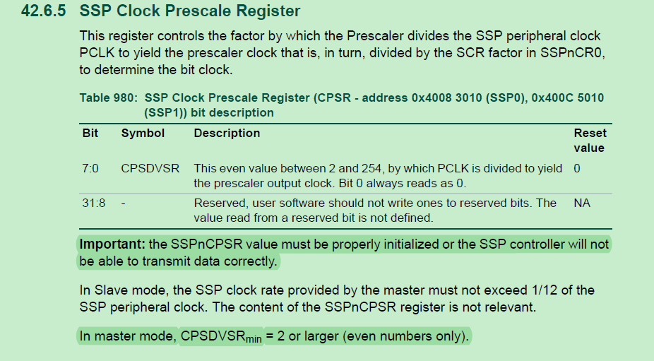
I am struggling to find the root problem, from the user manual, we can get that improper data in CPSDVSR will cause to transmit data incorrectly.
I will continue to check why 2 in CPSDVSR is not correct, any progress I will let you know.
Best Regards
Kerry
- Mark as New
- Bookmark
- Subscribe
- Mute
- Subscribe to RSS Feed
- Permalink
- Report Inappropriate Content
Thank you for the reply, I already have this example and I started from the periph_ssp example.
I am trying to do this in polling mode, I want to save interrupt time as well as DMA for other functions.
Can you get it to work in polling mode?
- Mark as New
- Bookmark
- Subscribe
- Mute
- Subscribe to RSS Feed
- Permalink
- Report Inappropriate Content
I just wanted to add. The waveform was generated after just writing 0x3A to DR register.
