- NXP Forums
- Product Forums
- General Purpose MicrocontrollersGeneral Purpose Microcontrollers
- i.MX Forumsi.MX Forums
- QorIQ Processing PlatformsQorIQ Processing Platforms
- Identification and SecurityIdentification and Security
- Power ManagementPower Management
- MCX Microcontrollers
- S32G
- S32K
- S32V
- MPC5xxx
- Other NXP Products
- Wireless Connectivity
- S12 / MagniV Microcontrollers
- Powertrain and Electrification Analog Drivers
- Sensors
- Vybrid Processors
- Digital Signal Controllers
- 8-bit Microcontrollers
- ColdFire/68K Microcontrollers and Processors
- PowerQUICC Processors
- OSBDM and TBDML
-
- Solution Forums
- Software Forums
- MCUXpresso Software and ToolsMCUXpresso Software and Tools
- CodeWarriorCodeWarrior
- MQX Software SolutionsMQX Software Solutions
- Model-Based Design Toolbox (MBDT)Model-Based Design Toolbox (MBDT)
- FreeMASTER
- eIQ Machine Learning Software
- Embedded Software and Tools Clinic
- S32 SDK
- S32 Design Studio
- Vigiles
- GUI Guider
- Zephyr Project
- Voice Technology
- Application Software Packs
- Secure Provisioning SDK (SPSDK)
- Processor Expert Software
-
- Topics
- Mobile Robotics - Drones and RoversMobile Robotics - Drones and Rovers
- NXP Training ContentNXP Training Content
- University ProgramsUniversity Programs
- Rapid IoT
- NXP Designs
- SafeAssure-Community
- OSS Security & Maintenance
- Using Our Community
-
-
- Home
- :
- Product Forums
- :
- S12 / MagniV Microcontrollers
- :
- questions about S12ZVM PWM dead-time settings and GDU external circuit design
questions about S12ZVM PWM dead-time settings and GDU external circuit design
- Subscribe to RSS Feed
- Mark Topic as New
- Mark Topic as Read
- Float this Topic for Current User
- Bookmark
- Subscribe
- Mute
- Printer Friendly Page
questions about S12ZVM PWM dead-time settings and GDU external circuit design
- Mark as New
- Bookmark
- Subscribe
- Mute
- Subscribe to RSS Feed
- Permalink
- Report Inappropriate Content
Description: Dear Sir,
My customer is using our S12ZM in their pump motor controller project(motor type is DC brush motor, so only 2 high sides and 2 low sides are used) and they meet issue of PWM dead-time settings and GDU external circuit design:
1. the dead-time setting of low side is correct while it’s much more shorter than the setting on high side: when set 1 us as the dead-time for both HS and LS, they measure about 0.4us dead-time on HS and about 1.05us on LS, is it normal, why it will has such huge difference on HS?
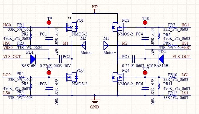
2. the customer adds a 33Ω resistor between S12ZVM GDU HSx/LSx and gate input pin of external power MOSFET, and also add a RC filter(R=470K and C=10nf) between gate and source of every power MOSFET for protection, which is necessary for their before products(use independent pre-driver, not integrated GDU as our S12ZVM): customer GDU external circuit is as below:
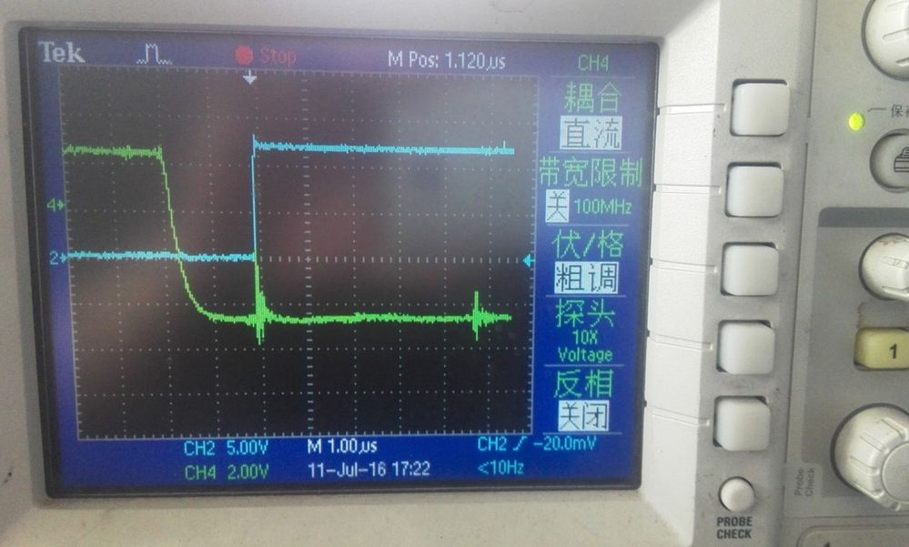
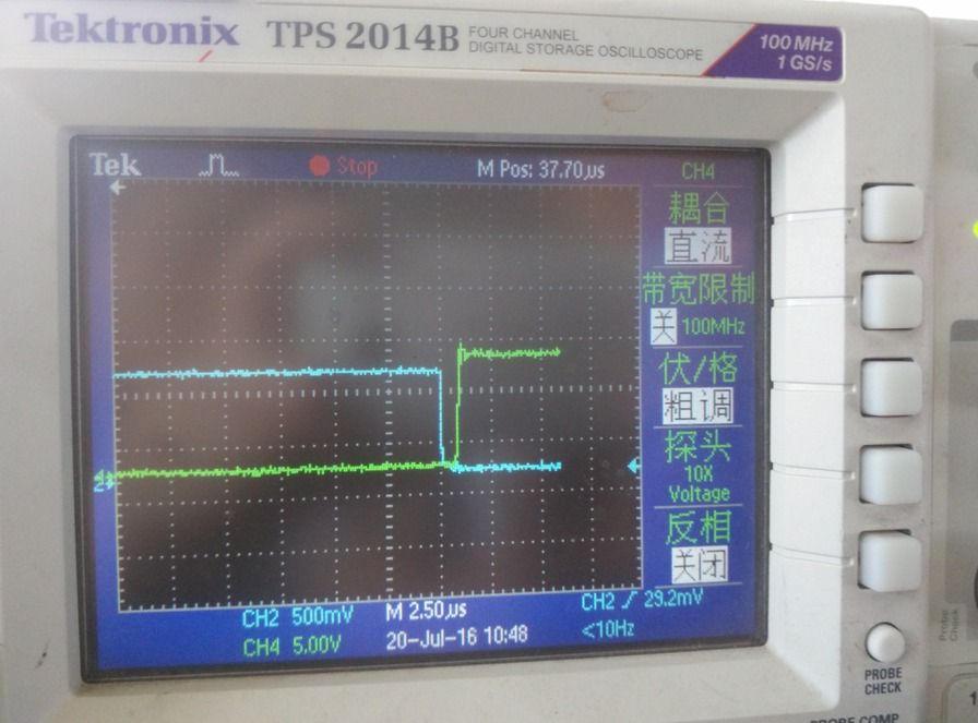
customer tests to find the 33 Ω serial resistor on MOSFET gate input will change S12ZVM GDU high side output HGx signal’s falling slope, make it become slow compare with LSx or without the resistor, while its rising slope is OK, also no such influence on LSx.(as below photo, set deadtime = 2us, the HSx is falling and LS is rising):

After remove the 33 Ω serial resistor, the HGx signal’s falling slope becomes normal.
How does this happen? Is it necessary to add the 33Ω serial resistor between S12ZVM GDU HSx/LSx and gate input pin of external power MOSFET, and the RC filter(R=470K and C=10nf) between gate and source of every power MOSFET for protection in S12ZM GDU application?
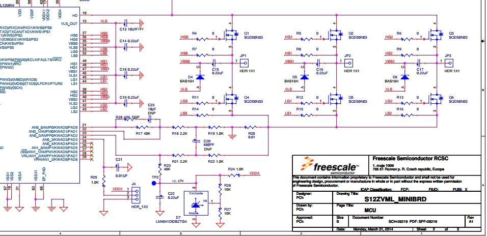
PS: I reviewed all our S12ZVM demo-boards and reference design, there is only a 0Ω serial resistor between S12ZVM GDU HSx/LSx and gate input pin of external power MOSFET and no the RC filter circuit between gate and source of every power MOSFET. attached schematic of S12ZVML_MINIBRD as below for your reference:
Best regard,
Enwei Hu.
- Mark as New
- Bookmark
- Subscribe
- Mute
- Subscribe to RSS Feed
- Permalink
- Report Inappropriate Content
Hi Enwei,
It depends on where you measure these dead-times.
The delay between PWM edge and transistor edge is typically calculated as:
Delay = TpreDRV+Ton/2+DT
While the predriver delay (TpreDRV) is typically 50ns, switching time of transistor (Ton) is typically 0.1~1.0us and the dead-time (DT) may be typically selected in range 0.3~4.0us.
I suppose that the PR2 (PR4/8/11) resistor (470k) is implemented here for safety reason. When we disconnect GDU driver from transistors, the resistor will discharge gate charge and close transistor.
Your scheme does not specify transistor type, however, I suppose that the RC circuit values given by PR1 and PC1 components are simply too big in compare with gate capacitance.
The PR1,PC1 time constant exactly fits with your result of the measurement. Tau= PR1*PC1 = 330ns.
I would like to recommend decrease PC1 (for example to 100pF) and PR1 (for example to 3.3Ohm) values. It will still influence your rising/falling slopes but in much smaller ratio.
In fact, RC circuits prior transistor gates are typically added for decreasing EMC radiation.
Fast edges = higher noise.
I hope it helps you.
Have a great day,
Radek
-----------------------------------------------------------------------------------------------------------------------
Note: If this post answers your question, please click the Correct Answer button. Thank you!
-----------------------------------------------------------------------------------------------------------------------
- Mark as New
- Bookmark
- Subscribe
- Mute
- Subscribe to RSS Feed
- Permalink
- Report Inappropriate Content
Hello Enwei,
Thanks for post your question on the community.
For the dead time please modify the Load mode register to: PMFCFG3_VLMODE=0b01; in this way we will be sure that the PMW time generator is the same for the three phases.
Also the values that you have on your RC filter are too high, for the RC filter we normally recommend a resistor of 100Ω and a capacitor of 4.7u, the 33Ohm resistor in HSx and LSx are not necessary, as normally these signals are used as reference, having a voltage dropped on the resistance is not the most optimal.
Please modify the values of your filter and any update just let me know.
Best regards,
- Mark as New
- Bookmark
- Subscribe
- Mute
- Subscribe to RSS Feed
- Permalink
- Report Inappropriate Content
Hi Radek and Alejandro,
Thank you very much for your reply on this issue. I have understood the relationship between actual measured deadtime and PWM module set, pre-driver(GDU) delay and extenral MOSFET turn on dely.
from our datasheet, when the PWM deadtime set 0, the GDU delay plus MOSFET turn-on dely will have a bout 0.2us addtional deadtime, so if we set PWM deadtime as 1us, the actual measured deadtime should be 1us + 0.2us== 1.2us:
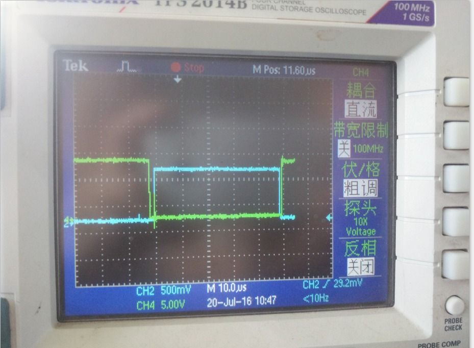
we set PMFCFG3_VLMODE=0b01 as you suggested(in fact, the PMFCFG3_VLMODE should be 0b00, for customer needs to control HSx and LSx PWM duty independently to drive the DC-brush motor move froward or inverse ), and measured the actual deadtime on our S12ZVML_MINIBRD , but the HSx deadtime is still 0.6us short than expected:
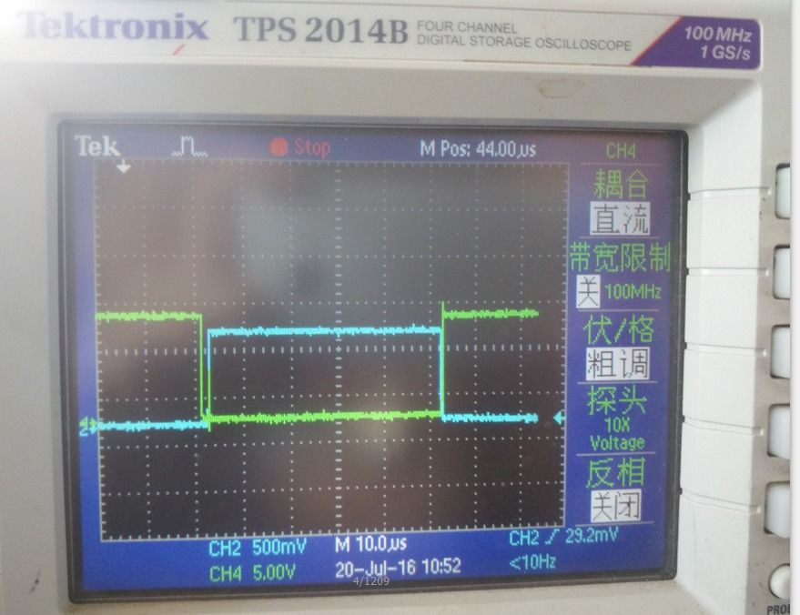
1. when we set PWM deadtime as 1.5us (HS is on Channel 2 and LSx is connected on Channel 4):
the deadtime on LSx is about 1.7us, and is OK:
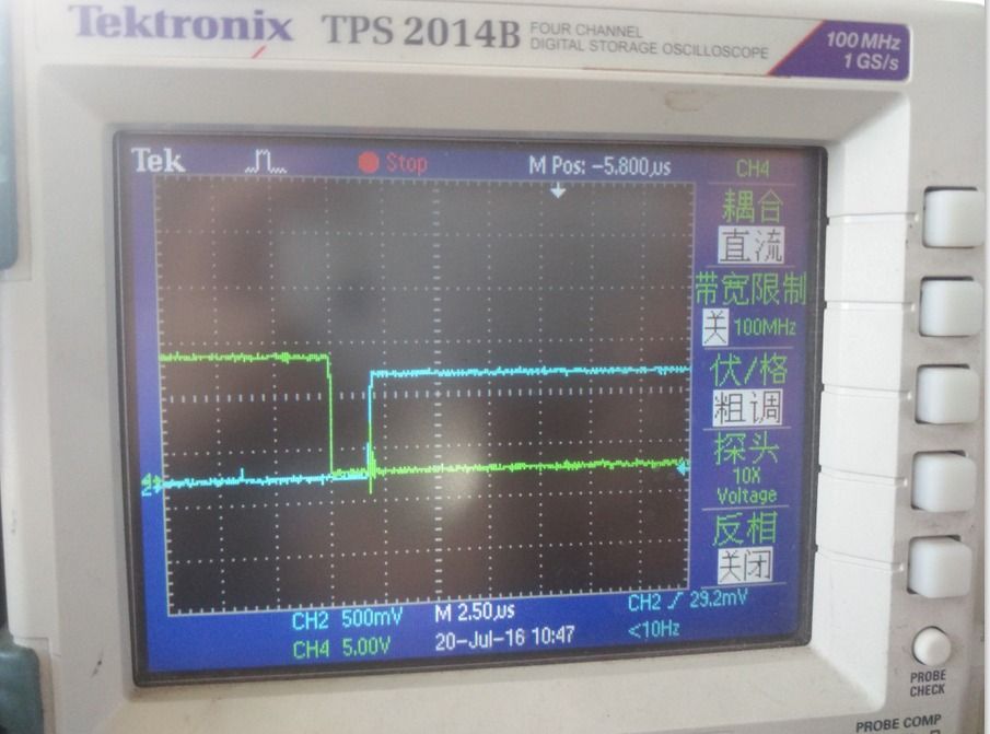
while the deadtime on HSx is only about 0.9us, it has about 0.6us delay when HSx falling from on to off:
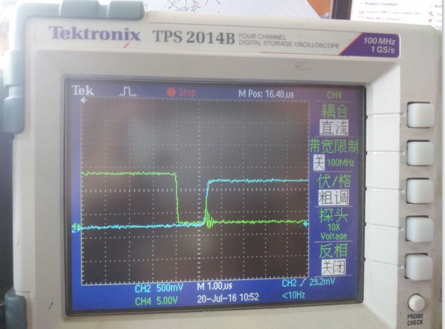
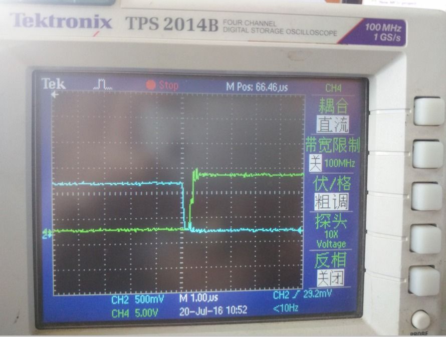
2. when we set PWM deadtime as 1us (HS is on Channel 2 and LSx is connected on Channel 4):
the deadtime on LSx is about 1.2us, and is OK:
while the deadtime on HSx while the deadtime on HSx is only about 0.4us, it still has about 0.6us delay whenHSx falling from on to off:
Why the HSx will always have 0.6us unexpected delay when drive it from high to low? and LSx has no such issue?
I think you can alos verify and repeat the issue on our demoboard, please help to explain the root cause.
Thanks~!
Best regard,
Enwei Hu
- Mark as New
- Bookmark
- Subscribe
- Mute
- Subscribe to RSS Feed
- Permalink
- Report Inappropriate Content
Hello Enwei,
Having the same time base (VLMODE=0b01) for the three phases doesn´t mean that you wont be able of control the velocity and direction of the motor.
For example, your time generator could be at 20kHz for the 6 pwm signals but you still having control of each duty cycle channel.
Regarding your graphs, are you measuring on HS0 and LS0? , on HS you have a voltage scale of 500mV and on LS you have a voltage scale of 5v??. In order to observe better the turn on/off of the Mosfet please measure directly on HG0 and LG0.
Also, could you share your PMF configuration, I run a brief test in our S12ZVM EVB with channel 0 and 1 in complementary mode and the dead time works properly.
Here is my example code: Core freq= 25MHz, PWM freq= 20kHz, Dead time= 2usec
Best regards,
Alejandro
