- NXP Forums
- Product Forums
- General Purpose MicrocontrollersGeneral Purpose Microcontrollers
- i.MX Forumsi.MX Forums
- QorIQ Processing PlatformsQorIQ Processing Platforms
- Identification and SecurityIdentification and Security
- Power ManagementPower Management
- MCX Microcontrollers
- S32G
- S32K
- S32V
- MPC5xxx
- Other NXP Products
- Wireless Connectivity
- S12 / MagniV Microcontrollers
- Powertrain and Electrification Analog Drivers
- Sensors
- Vybrid Processors
- Digital Signal Controllers
- 8-bit Microcontrollers
- ColdFire/68K Microcontrollers and Processors
- PowerQUICC Processors
- OSBDM and TBDML
-
- Solution Forums
- Software Forums
- MCUXpresso Software and ToolsMCUXpresso Software and Tools
- CodeWarriorCodeWarrior
- MQX Software SolutionsMQX Software Solutions
- Model-Based Design Toolbox (MBDT)Model-Based Design Toolbox (MBDT)
- FreeMASTER
- eIQ Machine Learning Software
- Embedded Software and Tools Clinic
- S32 SDK
- S32 Design Studio
- Vigiles
- GUI Guider
- Zephyr Project
- Voice Technology
- Application Software Packs
- Secure Provisioning SDK (SPSDK)
- Processor Expert Software
-
- Topics
- Mobile Robotics - Drones and RoversMobile Robotics - Drones and Rovers
- NXP Training ContentNXP Training Content
- University ProgramsUniversity Programs
- Rapid IoT
- NXP Designs
- SafeAssure-Community
- OSS Security & Maintenance
- Using Our Community
-
- Cloud Lab Forums
-
- Home
- :
- General Purpose Microcontrollers
- :
- Kinetis Microcontrollers
- :
- Questions on interfacing external SRAM & NAND Flash with MK60FN1M0
Questions on interfacing external SRAM & NAND Flash with MK60FN1M0
- Subscribe to RSS Feed
- Mark Topic as New
- Mark Topic as Read
- Float this Topic for Current User
- Bookmark
- Subscribe
- Mute
- Printer Friendly Page
Questions on interfacing external SRAM & NAND Flash with MK60FN1M0
- Mark as New
- Bookmark
- Subscribe
- Mute
- Subscribe to RSS Feed
- Permalink
- Report Inappropriate Content
Hi,
We are using MK60FN1M0 MCU and are planning to interface two memories: 8-bit SRAM and 8-bit NAND Flash. However, some of the pins are multiplexed between FlexBus and NFC, which in our case are NFC_WE/FB_RW and some FB address lines with NFC IO lines.
A block diagram showing the detailed connections is attached below.
My questions are:
1. Is the above block diagram realizable? Is there any scope to improve it?
2. If so, how does the FlexBus/NFC arbitration actually work?
In our application, we might need to access the second memory when the MCU is busy with one or we might need to transfer some data between memories through K60. For example: If K60 is writing/reading from NAND Flash and at the same time SRAM access is required, how will this be handled? Does the MCU automatically select the memory? If it is to be handled with application software, how do we handle this?
3. From where can we get the detailed description of SIM_SOPT6 register?
Any help is appreciated.
Thank you!
- Mark as New
- Bookmark
- Subscribe
- Mute
- Subscribe to RSS Feed
- Permalink
- Report Inappropriate Content
Hi
1> Yes, the block diagram is correct.
2> It is possible to access the SRAM and NAND as block diagram shows. Software doesn't need to take care of the arbitration, which hardware will do the arbitration work. Below with more detailed info about SIM_SOPT6 register PCR&MCC bits description:
PCR - Post-cycle reservation
Specifies the length of the FlexBus post-cycle reservation period in internal bus clock cycles.
0x0 or 0x1 No post-cycle reservation, and the arbiter returns to the idle loop as soon as the FlexBus is no longer busy.
0x2 or more Enables post-cycle reservation
MCC - Minimum consecutive cycles.
Specifies the minimum amount of time in internal bus clock cycles provided by the arbiter for NAND flash activity. At least MCC internal bus clock cycles must elapse before a FlexBus request is recognized, and the NFC may, in fact, use the shared pins for more than MCC internal bus clock cycles absent such a request. A value of 0 makes the arbiter respond immediately to a FlexBus request and pause the NFC as soon as possible.
In fact, my previous answer with some problem. The software just need to set the SIM_SOPT6 register as exptected.
Then software does not do anything to avoid access external SRAM and NAND Flash at same time (the hardware arbiter will do that job).
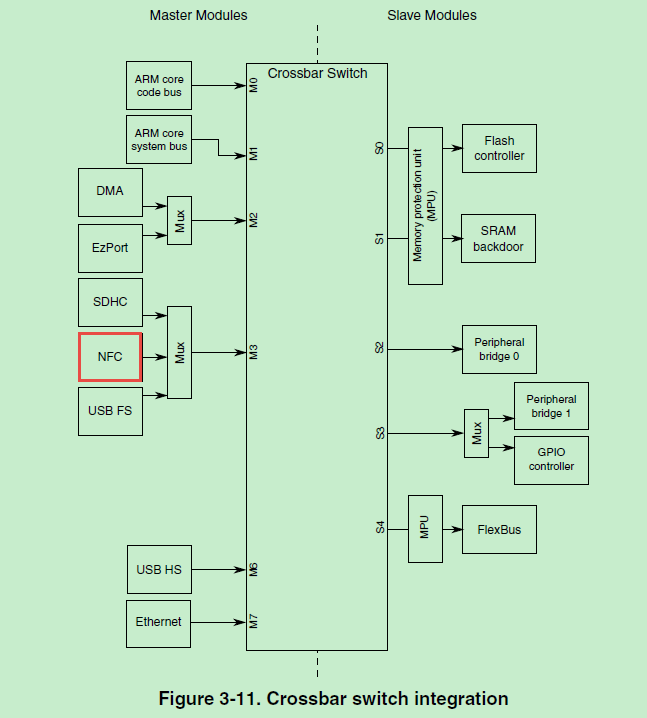
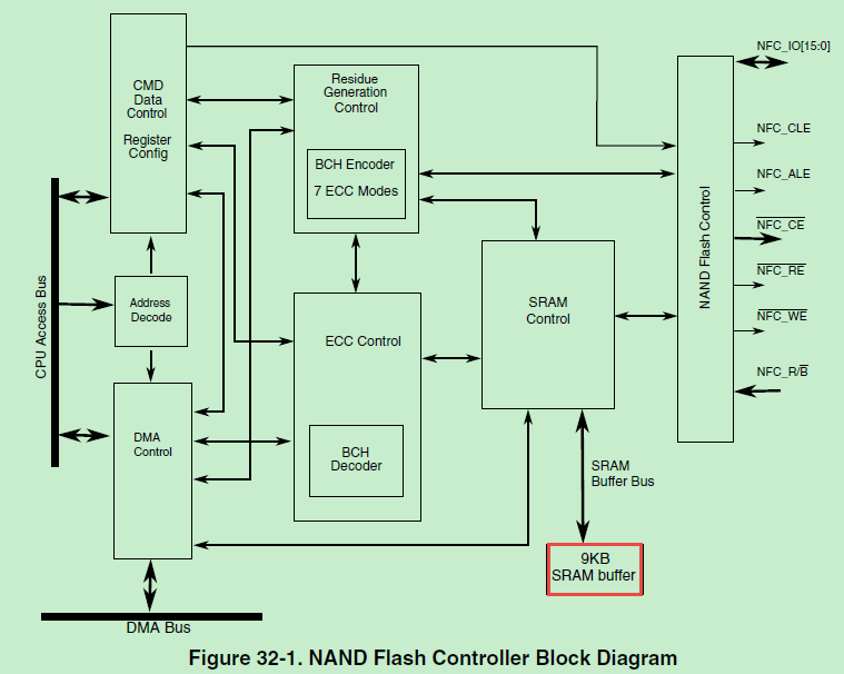
3> The crossbar setting without effection. For NFC as crossbar master doesn't have path to access Flexbus slave, which just could access 9KB SRAM buffer.
Wish it helps.
Have a great day,
Ma Hui
-----------------------------------------------------------------------------------------------------------------------
Note: If this post answers your question, please click the Correct Answer button. Thank you!
-----------------------------------------------------------------------------------------------------------------------
- Mark as New
- Bookmark
- Subscribe
- Mute
- Subscribe to RSS Feed
- Permalink
- Report Inappropriate Content
Hi,
(Note: I am replying from using my actual name/ new account now. I was using my colleague Hardik's account till now, as my old account is having some problems. Sorry for any inconvenience.)
Sorry for the delayed reply. Yes, it did help. Thank you so much for the further clarification with details, I really appreciate it. So, based on your answers, I think we will be able to go ahead with this memory interfacing.
However, I did not understand your answer no. 3 about the Crossbar Switch. Could you please explain the same again in some details? Can we think of using Crossbar Switch to help software with handling the external SRAM and NAND Flash memories or there is just no need for it?
Thanks & Regards.
- Mark as New
- Bookmark
- Subscribe
- Mute
- Subscribe to RSS Feed
- Permalink
- Report Inappropriate Content
Hi
The MK60FN1M0 reference manual shows NFC works as crossbar master 3 with below picture shows:
While, the NFC block diagram shows the NFC module could only access the 9KB SRAM buffer, there without other crossbar slave access interface provided to NFC module.
That's why I said Crossbar Configuration without any effect.
There doesn't need software code to manage Flexbus and NFC operation, those work was done by hardware.
Wish it helps.
Have a great day,
Ma Hui
-----------------------------------------------------------------------------------------------------------------------
Note: If this post answers your question, please click the Correct Answer button. Thank you!
-----------------------------------------------------------------------------------------------------------------------
- Mark as New
- Bookmark
- Subscribe
- Mute
- Subscribe to RSS Feed
- Permalink
- Report Inappropriate Content
Hi,
Thank you for the reply.
Ok, so...
1) You mean that NFC can only access 9KB SRAM buffer that is dedicated to it and it cannot access the FlexBus slave devices, correct?
2) Also, there is no need for software to modify/use Crossbar Switch registers for this particular interfacing case, correct?
Please confirm.
Thanks & Regards.
- Mark as New
- Bookmark
- Subscribe
- Mute
- Subscribe to RSS Feed
- Permalink
- Report Inappropriate Content
Hi
Yes, both are correct.
Wish it helps.
Have a great day,
Ma Hui
-----------------------------------------------------------------------------------------------------------------------
Note: If this post answers your question, please click the Correct Answer button. Thank you!
-----------------------------------------------------------------------------------------------------------------------
- Mark as New
- Bookmark
- Subscribe
- Mute
- Subscribe to RSS Feed
- Permalink
- Report Inappropriate Content
Hi,
Okay, thanks so much for your time and help.
Have a great day.
Thanks & Regards,
Kaitav
- Mark as New
- Bookmark
- Subscribe
- Mute
- Subscribe to RSS Feed
- Permalink
- Report Inappropriate Content
Hi
1> I checked attached MCU-Memory interfacing block diagram without any problem.
2> K60 does implement an arbitration scheme that allows for sharing between the FlexBus and NFC; however, this sharing is really only used for the NFC data lines/FlexBus AD lines and the NFC_WE and FlexBus R/W signals. If you look at the signal muxing table in the manual you can see that these pins only have a single function selection for FlexBus/NFC. For example, PTB20 function ALT5 is “FB_AD31/NFC_DATA15.” So this is a case where the pin is configured for a FB/NFC mode and dynamically switches between the two.
So customer application software should avoid to access SRAM and NAND Flash at same time.
3> The SIM_SOPT6 register has two settings that are related to how long the the FlexBus or Nand Flash Controller (NFC) will hold the bus before giving it up to the other. PCR - FlexBus hold cycles before FlexBus can release bus to NFC or to IDLE. MCC - NFC hold cycle in case FlexBus request while NFC is granted.
Wish it helps.
Have a great day,
Ma Hui
-----------------------------------------------------------------------------------------------------------------------
Note: If this post answers your question, please click the Correct Answer button. Thank you!
-----------------------------------------------------------------------------------------------------------------------
- Mark as New
- Bookmark
- Subscribe
- Mute
- Subscribe to RSS Feed
- Permalink
- Report Inappropriate Content
Hi Ma Hui,
Thank you for the answers. I still want to clarify a few things with respect to your reply.
1) Just to confirm: Does it mean that we can go ahead and covert the block diagram into a full schematic? The block diagram is correct, right?
2) Yes, I understand that NFC and FlexBus are multiplexed and that only one will work at one point. But you can see in the block diagram that the signals we are using are on the same ALT functionality. That is, they are muxed on the same ALT pins and we can only access only one peripheral (NAND or SRAM) at a time. But if it is possible to interface both NAND and SRAM to the MCU as shown in the block diagram, how does software take care of the arbitration? What care do we need to take in software so that MCU accesses only one at a time?
3) Is there any chance we can make use of Crossbar Switch in the software to work with these memories?
Your reply will be highly appreciable.
Thanks & Regards.
- Mark as New
- Bookmark
- Subscribe
- Mute
- Subscribe to RSS Feed
- Permalink
- Report Inappropriate Content
Anyone please?
- Mark as New
- Bookmark
- Subscribe
- Mute
- Subscribe to RSS Feed
- Permalink
- Report Inappropriate Content
Dave,
Can't help you directly on the FlexBus connection as I've not used it. However, when you ask for information on the SIM_SOPT6 register that makes me wonder have you read the reference manual for the K60? Not the datasheet, but the reference manual. This will also give you a lot of info on Flexbus. Essential reading.
http://cache.nxp.com/files/32bit/doc/ref_manual/K60P144M100SF2V2RM.pdf
- Mark as New
- Bookmark
- Subscribe
- Mute
- Subscribe to RSS Feed
- Permalink
- Report Inappropriate Content
Hi Petec,
Thanks for the reply.
Yes, I have already read the reference manual and the FlexBus chapter a few times now. The manual is lacking the description of SIM_SOPT6 register, which is why I have asked for more details. I did get some information about this register from some other thread anyway, but I have still not fully understood how the FlexBus/NFC arbitration is done.
My only questions are the ones I have mentioned above. The attached block diagram shows that our block level schematic is also ready. Just need the assure that all of this would work well when we implement it.
Regards.

