- NXP Forums
- Product Forums
- General Purpose MicrocontrollersGeneral Purpose Microcontrollers
- i.MX Forumsi.MX Forums
- QorIQ Processing PlatformsQorIQ Processing Platforms
- Identification and SecurityIdentification and Security
- Power ManagementPower Management
- MCX Microcontrollers
- S32G
- S32K
- S32V
- MPC5xxx
- Other NXP Products
- Wireless Connectivity
- S12 / MagniV Microcontrollers
- Powertrain and Electrification Analog Drivers
- Sensors
- Vybrid Processors
- Digital Signal Controllers
- 8-bit Microcontrollers
- ColdFire/68K Microcontrollers and Processors
- PowerQUICC Processors
- OSBDM and TBDML
-
- Solution Forums
- Software Forums
- MCUXpresso Software and ToolsMCUXpresso Software and Tools
- CodeWarriorCodeWarrior
- MQX Software SolutionsMQX Software Solutions
- Model-Based Design Toolbox (MBDT)Model-Based Design Toolbox (MBDT)
- FreeMASTER
- eIQ Machine Learning Software
- Embedded Software and Tools Clinic
- S32 SDK
- S32 Design Studio
- Vigiles
- GUI Guider
- Zephyr Project
- Voice Technology
- Application Software Packs
- Secure Provisioning SDK (SPSDK)
- Processor Expert Software
-
- Topics
- Mobile Robotics - Drones and RoversMobile Robotics - Drones and Rovers
- NXP Training ContentNXP Training Content
- University ProgramsUniversity Programs
- Rapid IoT
- NXP Designs
- SafeAssure-Community
- OSS Security & Maintenance
- Using Our Community
-
-
- Home
- :
- Product Forums
- :
- S12 / MagniV Microcontrollers
- :
- How can i find the result of Supply Voltage Sensor in MC9S12VR Chip?
How can i find the result of Supply Voltage Sensor in MC9S12VR Chip?
- Subscribe to RSS Feed
- Mark Topic as New
- Mark Topic as Read
- Float this Topic for Current User
- Bookmark
- Subscribe
- Mute
- Printer Friendly Page
How can i find the result of Supply Voltage Sensor in MC9S12VR Chip?
- Mark as New
- Bookmark
- Subscribe
- Mute
- Subscribe to RSS Feed
- Permalink
- Report Inappropriate Content
I am using the MC9S12VR family chip for WR.
I know it is having Supply Voltage Sensor and Chip temperature sensor AD Special channel.
But i cannot find the Conversion Result Registers of Supply Voltage Sensor(Chapter 16) and Chip temperature sensor(section 4.3.2.13) in Datesheet.
Someone can help to explain for me?
Thank you very much!
- Mark as New
- Bookmark
- Subscribe
- Mute
- Subscribe to RSS Feed
- Permalink
- Report Inappropriate Content
Hi Juejie,
The Conversion Result Registers is the same for all ADC measurements - ATDDR0~ATDDR5.
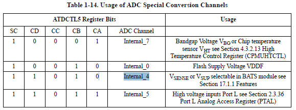
The internal channels are routed to ADC by setting SC bit in ATDCTL5 register.
Please look at Table 1-14. Usage of ADC Special Conversion Channels in RM (page 51, RM Rev4.2) for channel settings of internal channels.
So, the Bandgap Voltage VBG or Chip temperature sensor VHT are measured on Internal_7 channel and VSENSE or VSUP voltage is measured on Internal_4 channel.
Prior ADC measurement, you have to also configure the appropriate module. For example:
CPMUHTCTL=0x08; // temperature VHT signal, the voltage amplifier is enabled
Or
BATE=0x08; // BATS VSUP ADC Connection Enable
I hope it helps you.
Have a great day,
RadekS
-----------------------------------------------------------------------------------------------------------------------
Note: If this post answers your question, please click the Correct Answer button. Thank you!
-----------------------------------------------------------------------------------------------------------------------
- Mark as New
- Bookmark
- Subscribe
- Mute
- Subscribe to RSS Feed
- Permalink
- Report Inappropriate Content
Hi Radek
Thanks very much for your detail explain!
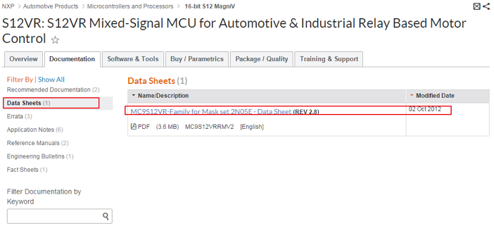
It looks like some mistakes in "MC9S12VR Family Reference Manual, Rev. 2.8". I hope official team can update this information ASAP.
But I still have a query about the Conversion Result Registers.
If i use the Multi-Channel Sample Mode (MULT = 1),scan mode(SCAN = 1) and enable the AN0, AN1, Supply Voltage Sensor and Chip temperature sensor.
How the Conversion Result Registers will be allotted for all ADC channels?
In my mind, the allocation as following:
ATDDR0 --> AN0
ATDDR1 --> AN1
ATDDR2 --> Internal_4
ATDDR3 --> Internal_7
Is it correct?
And If i enable the AN0~AN5, Supply Voltage Sensor and Chip temperature sensor.
In this case how the ATDDR0~ATDDR5 will be allotted ?
Thanks again!
- Mark as New
- Bookmark
- Subscribe
- Mute
- Subscribe to RSS Feed
- Permalink
- Report Inappropriate Content
Hi Juejie,
Unfortunately, the ATD module isn’t such flexible in channel selection.
SC bit in ATDCTL5 register selects whether you will measure internal or external channels. So, you cannot measure AN0 together with Internal_4 channel in continuous mode.
You may measure AN0~AN5 with results in ATDDR0~ATDDR5 registers or Internal _7..Internal_5 channels with results in ATDDR0~ATDDR5 registers.
In fact, I am not sure how internal channel results will be sorted when you select Multi-Channel Sample Continuous mode –I never test it. I used just single channel one shot measurement (result will be always in ATDDR0).
I hope it helps you.
Have a great day,
RadekS
-----------------------------------------------------------------------------------------------------------------------
Note: If this post answers your question, please click the Correct Answer button. Thank you!
-----------------------------------------------------------------------------------------------------------------------

