- NXP Forums
- Product Forums
- General Purpose MicrocontrollersGeneral Purpose Microcontrollers
- i.MX Forumsi.MX Forums
- QorIQ Processing PlatformsQorIQ Processing Platforms
- Identification and SecurityIdentification and Security
- Power ManagementPower Management
- MCX Microcontrollers
- S32G
- S32K
- S32V
- MPC5xxx
- Other NXP Products
- Wireless Connectivity
- S12 / MagniV Microcontrollers
- Powertrain and Electrification Analog Drivers
- Sensors
- Vybrid Processors
- Digital Signal Controllers
- 8-bit Microcontrollers
- ColdFire/68K Microcontrollers and Processors
- PowerQUICC Processors
- OSBDM and TBDML
-
- Solution Forums
- Software Forums
- MCUXpresso Software and ToolsMCUXpresso Software and Tools
- CodeWarriorCodeWarrior
- MQX Software SolutionsMQX Software Solutions
- Model-Based Design Toolbox (MBDT)Model-Based Design Toolbox (MBDT)
- FreeMASTER
- eIQ Machine Learning Software
- Embedded Software and Tools Clinic
- S32 SDK
- S32 Design Studio
- Vigiles
- GUI Guider
- Zephyr Project
- Voice Technology
- Application Software Packs
- Secure Provisioning SDK (SPSDK)
- Processor Expert Software
-
- Topics
- Mobile Robotics - Drones and RoversMobile Robotics - Drones and Rovers
- NXP Training ContentNXP Training Content
- University ProgramsUniversity Programs
- Rapid IoT
- NXP Designs
- SafeAssure-Community
- OSS Security & Maintenance
- Using Our Community
-
-
- Home
- :
- Product Forums
- :
- Vybrid Processors
- :
- Configurable interval of DMA_ACT of Vybrid.
Configurable interval of DMA_ACT of Vybrid.
- Subscribe to RSS Feed
- Mark Topic as New
- Mark Topic as Read
- Float this Topic for Current User
- Bookmark
- Subscribe
- Mute
- Printer Friendly Page
Configurable interval of DMA_ACT of Vybrid.
- Mark as New
- Bookmark
- Subscribe
- Mute
- Subscribe to RSS Feed
- Permalink
- Report Inappropriate Content
HI community.
Our customer has question below.
About the configurable interval of DMA_ACT.
Is it correct my understanding of the below comments.
Vybrid RM description .
57.5.10 DMA and De-interlace
After doing some necessary register configuration, such as coefficients, INVSZ and
DMA_ADDR, user can activate DMA by setting the DMA_ACT of the status and
configuration register. But note that DMA_ACT can be configured only during vertical
blanking since the VIU3 block will not transfer a fragment of video field to memory. If it
is configured during field active time, DMA transfer cannot be started and an error
interrupt will be asserted.
<Question>
Specifically, it can be set " 1 " to DMA_ACT , It is only within the interrupt handler by DMA_END_IRQ( Transfer the end of the video period) , and in the interrupt handler by VSYNC_IRQ .
.
- Mark as New
- Bookmark
- Subscribe
- Mute
- Subscribe to RSS Feed
- Permalink
- Report Inappropriate Content
Dear Karina- san,
Thank you for reply.
When is a way that had you suggested,
- Access occurs in the DDR memory in spite of not display.
- Applications and DCU can use at 2frames.(1 → 2,2 → 3.3 begins overwritten with the new data by past the discard.)
The above is the understanding. However, please suggest the best method from the following reasons.
- Even without access to the buffer of discard, I want to as long as possible time that can be used in other than the VIU
- Simply may be increased buffer, but the use of RAM has been tight, want to reduce as much as possible.
<Question>
Without the buffer access for discard, Is there a way to throw away.
(For example. If throw away, as it is allowed to stand without DMA_ACT,did on the process in the next Vysnc, I can use a method such as the DMA_ACT.
- Mark as New
- Bookmark
- Subscribe
- Mute
- Subscribe to RSS Feed
- Permalink
- Report Inappropriate Content
takashitakahashi did you get previous update?
- Mark as New
- Bookmark
- Subscribe
- Mute
- Subscribe to RSS Feed
- Permalink
- Report Inappropriate Content
jiri-b36968 FYI
- Mark as New
- Bookmark
- Subscribe
- Mute
- Subscribe to RSS Feed
- Permalink
- Report Inappropriate Content
Hello Takashi-san,
not sure if I understand:
You want to display every second frame. De-interlace?
so you should ignore every second framer.
Not sure how your driver does it, but you can do it for example like this:
Ext image transfer address
1 buffer [0] display
2 buffer [1] discard
3 buffer [1] display
4 buffer [0] discard
5 buffer [0] display
/Jiri
- Mark as New
- Bookmark
- Subscribe
- Mute
- Subscribe to RSS Feed
- Permalink
- Report Inappropriate Content
Dear Jiri-san.
Thank you for your replay.
I have about external input image format question.
For external input, transfer control of 2nd image.
[b] 1(1st) image transfer completed and the buffer address setting after the next 2nd image transfer restart.
External has been received to 60fps (every 16.6ms) from, but we would like to thinning as follows without changing the input from the outside.
-------------------------------------------------- ------------------------------------------------------------------------
External image ① ② ③ ④ ⑤
Transfer start address buffer [0] discard buffer [1] discard buffer [2]
-------------------------------------------------- --------------------------------------------------------------------------
As the implementation method, we thought should be the control of the [b] at the time of an odd number of times of Vsync interrupt.
But, remaining data that was not received in an even number of times is in the FIFO, and is concerned that than would wreckage of the data is entered into the next buffer.
Could you suggest the implementation method.
- Mark as New
- Bookmark
- Subscribe
- Mute
- Subscribe to RSS Feed
- Permalink
- Report Inappropriate Content
jiri-b36968 can you share your comments?
- Mark as New
- Bookmark
- Subscribe
- Mute
- Subscribe to RSS Feed
- Permalink
- Report Inappropriate Content
Hi Takashi,
From the DMA and De-interlace (57.5.10) and Initialization Information(57.6) description, It's looks like DMA_ACT bit(27th bit field) can be set by using VIU3_SCR Configuration Register to start FIFO and DMA transfer. So this operation actually starts the VIU3 to operate.
The DMA_ACT bit is not within the DMA_END_IRQ interrupt handler instead "DMA_ACT" is part of VIU3 Status And Configuration Register bit(VIU3_SCR).
You could refer the 57.6.1 Initialization Information from the following vybrid reference manual link for more information.
Thanks,
Timesys Support
- Mark as New
- Bookmark
- Subscribe
- Mute
- Subscribe to RSS Feed
- Permalink
- Report Inappropriate Content
Hi community.
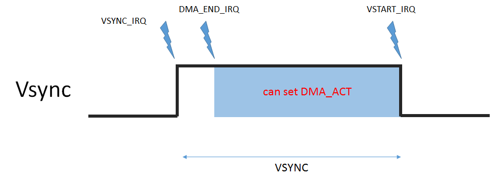
As RM explains that DMA_ACT should be set during VSYNC period.
My understanding is that VSYNC_IRQ is set at start point of VSYNC and VSTART_IRQ is set at end of VSYNC.
I guess DMA_END_IRQ is set within VSYNC.
So My understanding is that DMA_ACT can set between DMA_END_IRQ and VSTART. Could you confirm it ?
This is HW question, so please include HW team, too.
- Mark as New
- Bookmark
- Subscribe
- Mute
- Subscribe to RSS Feed
- Permalink
- Report Inappropriate Content
- Mark as New
- Bookmark
- Subscribe
- Mute
- Subscribe to RSS Feed
- Permalink
- Report Inappropriate Content
Hello Takashi-san,
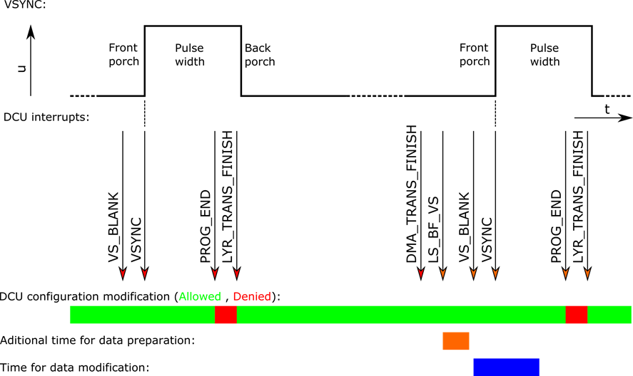
Transfer of layer configuration registers have to be done at proper moment.
Flags and interrupt sources are available and have to be used.
It is not allowed to attempt registers during transfer of configuration into DCU logic.
More here: please look at DCU_layer_transfer_issue_3.pdf just uploaded.
/Jiri
- Mark as New
- Bookmark
- Subscribe
- Mute
- Subscribe to RSS Feed
- Permalink
- Report Inappropriate Content
timesyssupport can you help here?

