- NXP Forums
- Product Forums
- General Purpose MicrocontrollersGeneral Purpose Microcontrollers
- i.MX Forumsi.MX Forums
- QorIQ Processing PlatformsQorIQ Processing Platforms
- Identification and SecurityIdentification and Security
- Power ManagementPower Management
- MCX Microcontrollers
- S32G
- S32K
- S32V
- MPC5xxx
- Other NXP Products
- Wireless Connectivity
- S12 / MagniV Microcontrollers
- Powertrain and Electrification Analog Drivers
- Sensors
- Vybrid Processors
- Digital Signal Controllers
- 8-bit Microcontrollers
- ColdFire/68K Microcontrollers and Processors
- PowerQUICC Processors
- OSBDM and TBDML
-
- Solution Forums
- Software Forums
- MCUXpresso Software and ToolsMCUXpresso Software and Tools
- CodeWarriorCodeWarrior
- MQX Software SolutionsMQX Software Solutions
- Model-Based Design Toolbox (MBDT)Model-Based Design Toolbox (MBDT)
- FreeMASTER
- eIQ Machine Learning Software
- Embedded Software and Tools Clinic
- S32 SDK
- S32 Design Studio
- Vigiles
- GUI Guider
- Zephyr Project
- Voice Technology
- Application Software Packs
- Secure Provisioning SDK (SPSDK)
- Processor Expert Software
-
- Topics
- Mobile Robotics - Drones and RoversMobile Robotics - Drones and Rovers
- NXP Training ContentNXP Training Content
- University ProgramsUniversity Programs
- Rapid IoT
- NXP Designs
- SafeAssure-Community
- OSS Security & Maintenance
- Using Our Community
-
- Cloud Lab Forums
-
- Home
- :
- General Purpose Microcontrollers
- :
- Kinetis Microcontrollers
- :
- Unreliable J-link flashing to KL16
Unreliable J-link flashing to KL16
- Subscribe to RSS Feed
- Mark Topic as New
- Mark Topic as Read
- Float this Topic for Current User
- Bookmark
- Subscribe
- Mute
- Printer Friendly Page
- Mark as New
- Bookmark
- Subscribe
- Mute
- Subscribe to RSS Feed
- Permalink
- Report Inappropriate Content
In a previously working configuration, I can't seem to successfully flash. I see "block verification error" and "Can not read register 0 (R0) while CPU is running". Any thoughts?
SEGGER J-Link GDB Server V4.98b Command Line Version
JLinkARM.dll V4.98b (DLL compiled Apr 10 2015 20:35:16)
-----GDB Server start settings-----
GDBInit file: none
GDB Server Listening port: 2331
SWO raw output listening port: 2332
Terminal I/O port: 2333
Accept remote connection: localhost only
Generate logfile: off
Verify download: on
Init regs on start: on
Silent mode: off
Single run mode: on
Target connection timeout: 0 ms
------J-Link related settings------
J-Link Host interface: USB
J-Link script: none
J-Link settings file: none
------Target related settings------
Target device: MKL16Z128xxx4
Target interface: SWD
Target interface speed: 1000kHz
Target endian: little
Connecting to J-Link...
J-Link is connected.
Firmware: J-Link V9 compiled Mar 2 2016 14:43:29
Hardware: V9.30
S/N: 59306698
Feature(s): GDB
Checking target voltage...
Target voltage: 1.83 V
Listening on TCP/IP port 2331
Connecting to target...Connected to target
Waiting for GDB connection...Connected to 127.0.0.1
Reading all registers
Read 4 bytes @ address 0x00000000 (Data = 0x20003000)
Target interface speed set to 1000 kHz
Resetting target
Halting target CPU...
...Target halted (PC = 0x0000A934)
R0 = FFFFFFFF, R1 = F000300C, R2 = 00000400, R3 = 20003000
R4 = FFFFFFFF, R5 = 00000000, R6 = 000000FF, R7 = 1FFFF161
R8 = FBFFF2FF, R9 = FF6FFFE7, R10= FFFF6EFF, R11= BFFFFFFD
R12= BDEFBFFC, R13= 20003000, MSP= 20003000, PSP= FFDFF77C
R14(LR) = FFFFFFF9, R15(PC) = 0000A934
XPSR A1000000, APSR A0000000, EPSR 01000000, IPSR 00000000
CFBP 00000000, CONTROL 00, FAULTMASK 00, BASEPRI 00, PRIMASK 00
Reading all registers
Target interface speed set to 1000 kHz
Flash breakpoints enabled
Semi-hosting enabled (VectorAddr = 0x08)
Semihosting I/O set to TELNET Client
SWO disabled succesfully.
SWO enabled succesfully.
Downloading 192 bytes @ address 0x00000000 - Verified OK
Downloading 16000 bytes @ address 0x00000410 - Verified OK
Downloading 15856 bytes @ address 0x00004290 - Verified OK
Downloading 16048 bytes @ address 0x00008080 - Verified OK
Downloading 16240 bytes @ address 0x0000BF30 - Verified OK
Downloading 16240 bytes @ address 0x0000FEA0 - Verified OK
Downloading 900 bytes @ address 0x00013E10 - Verified OK
Downloading 8 bytes @ address 0x00014194 - Verified OK
Downloading 8 bytes @ address 0x0001419C - Verified OK
Downloading 4 bytes @ address 0x000141A4 - Verified OK
Downloading 112 bytes @ address 0x000141A8 - Verified OK
Downloading 24 bytes @ address 0x00014218 - Verified OK
Read 4 bytes @ address 0x0000A934 (Data = 0x1C184B09)
Read 2 bytes @ address 0x0000A41A (Data = 0xF7FF)
Read 2 bytes @ address 0x0000A41A (Data = 0xF7FF)
Comparing flash [....................] Done.
Erasing flash [....................] Done.
Programming flash [....................] Done.
ERROR: Programming failed @ address 0x0000A400 (block verification error)
Verifying flash [....................] Done.
Resetting target
Halting target CPU...
...Target halted (PC = 0x0000A934)
Read 2 bytes @ address 0x0000A41A (Data = 0xF7FF)
Read 2 bytes @ address 0x0000A41A (Data = 0xF7FF)
Read 2 bytes @ address 0x0000A41A (Data = 0xF7FF)
R0 = 00000050, R1 = F000300C, R2 = 0000A400, R3 = 00000200
R4 = BD38601A, R5 = 00000000, R6 = 000000FF, R7 = 1FFFF161
R8 = FBFFF2FF, R9 = FF6FFFE7, R10= FFFF6EFF, R11= BFFFFFFD
R12= BDEFBFFC, R13= 20003000, MSP= 20003000, PSP= FFDFF77C
R14(LR) = 1FFFF159, R15(PC) = 0000A934
XPSR 01000000, APSR 00000000, EPSR 01000000, IPSR 00000000
CFBP 00000000, CONTROL 00, FAULTMASK 00, BASEPRI 00, PRIMASK 00
Reading all registers
Read 4 bytes @ address 0x0000A934 (Data = 0x1C184B09)
Setting breakpoint @ address 0x0000A41A, Size = 2, BPHandle = 0x0002
Starting target CPU...
ERROR: Can not read register 15 (R15) while CPU is running
...Target halted (PC = 0x00000000)
Reading all registers
ERROR: Can not read register 0 (R0) while CPU is running
ERROR: Can not read register 1 (R1) while CPU is running
ERROR: Can not read register 2 (R2) while CPU is running
ERROR: Can not read register 3 (R3) while CPU is running
ERROR: Can not read register 4 (R4) while CPU is running
ERROR: Can not read register 5 (R5) while CPU is running
ERROR: Can not read register 6 (R6) while CPU is running
ERROR: Can not read register 7 (R7) while CPU is running
ERROR: Can not read register 8 (R8) while CPU is running
ERROR: Can not read register 9 (R9) while CPU is running
ERROR: Can not read register 10 (R10) while CPU is running
ERROR: Can not read register 11 (R11) while CPU is running
ERROR: Can not read register 12 (R12) while CPU is running
ERROR: Can not read register 13 (R13) while CPU is running
ERROR: Can not read register 14 (R14) while CPU is running
ERROR: Can not read register 15 (R15) while CPU is running
ERROR: Can not read register 16 (XPSR) while CPU is running
ERROR: Can not read register 17 (MSP) while CPU is running
ERROR: Can not read register 18 (PSP) while CPU is running
ERROR: Can not read register 24 (PRIMASK) while CPU is running
ERROR: Can not read register 25 (BASEPRI) while CPU is running
ERROR: Can not read register 26 (FAULTMASK) while CPU is running
ERROR: Can not read register 27 (CONTROL) while CPU is running
Removing breakpoint @ address 0x0000A41A, Size = 2
WARNING: Failed to read memory @ address 0x00000000
Read 4 bytes @ address 0x00000000 (Data = 0x20003000)
Solved! Go to Solution.
- Mark as New
- Bookmark
- Subscribe
- Mute
- Subscribe to RSS Feed
- Permalink
- Report Inappropriate Content
Hi Jacob,
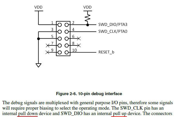
The SWD_CLK pin has an internal pull down and SWD_DIO has an internal pull up. But an external 4.7 kΩ to 10 kΩ pullup is recommended on SWD_DIO. You can refer the 10-pin debug interface below.
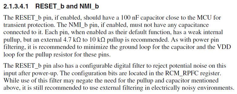
And the RESET_b and NMI_b should be care.
Best Regards,
Robin
- Mark as New
- Bookmark
- Subscribe
- Mute
- Subscribe to RSS Feed
- Permalink
- Report Inappropriate Content
Resolved: Needed 10k pullup on SWD clk and SWD reset, pulldown on clock

