- NXP Forums
- Product Forums
- General Purpose MicrocontrollersGeneral Purpose Microcontrollers
- i.MX Forumsi.MX Forums
- QorIQ Processing PlatformsQorIQ Processing Platforms
- Identification and SecurityIdentification and Security
- Power ManagementPower Management
- MCX Microcontrollers
- S32G
- S32K
- S32V
- MPC5xxx
- Other NXP Products
- Wireless Connectivity
- S12 / MagniV Microcontrollers
- Powertrain and Electrification Analog Drivers
- Sensors
- Vybrid Processors
- Digital Signal Controllers
- 8-bit Microcontrollers
- ColdFire/68K Microcontrollers and Processors
- PowerQUICC Processors
- OSBDM and TBDML
-
- Solution Forums
- Software Forums
- MCUXpresso Software and ToolsMCUXpresso Software and Tools
- CodeWarriorCodeWarrior
- MQX Software SolutionsMQX Software Solutions
- Model-Based Design Toolbox (MBDT)Model-Based Design Toolbox (MBDT)
- FreeMASTER
- eIQ Machine Learning Software
- Embedded Software and Tools Clinic
- S32 SDK
- S32 Design Studio
- Vigiles
- GUI Guider
- Zephyr Project
- Voice Technology
- Application Software Packs
- Secure Provisioning SDK (SPSDK)
- Processor Expert Software
-
- Topics
- Mobile Robotics - Drones and RoversMobile Robotics - Drones and Rovers
- NXP Training ContentNXP Training Content
- University ProgramsUniversity Programs
- Rapid IoT
- NXP Designs
- SafeAssure-Community
- OSS Security & Maintenance
- Using Our Community
-
-
- Home
- :
- General Purpose Microcontrollers
- :
- Kinetis Microcontrollers
- :
- K64F ADC - Using a 3.3V voltage reference IC as VREFH, with VDDA = 3.3V from a seperate power supply
K64F ADC - Using a 3.3V voltage reference IC as VREFH, with VDDA = 3.3V from a seperate power supply
- Subscribe to RSS Feed
- Mark Topic as New
- Mark Topic as Read
- Float this Topic for Current User
- Bookmark
- Subscribe
- Mute
- Printer Friendly Page
K64F ADC - Using a 3.3V voltage reference IC as VREFH, with VDDA = 3.3V from a seperate power supply
- Mark as New
- Bookmark
- Subscribe
- Mute
- Subscribe to RSS Feed
- Permalink
- Report Inappropriate Content
Hi,
In the K64F datasheet, it is specified that:
Max VREFH = VDDA.
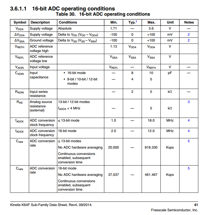
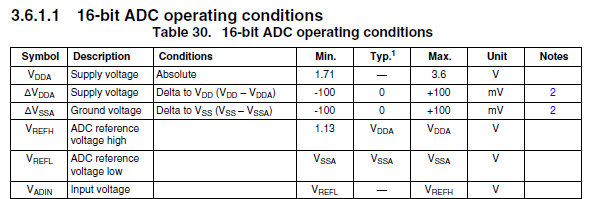
(See figure 3.6.1.1)
In our application, VREFH is connected to an external 3.3V voltage reference IC (LM4120AIM5-3.3), and VDDA is supplied by a separate 3.3V power supply IC (MAX8881EUT33-T). What are the repercussions in situations where VDDA is lower than VREFH(due to the fluctuations in line regulation of both chips)?
- Mark as New
- Bookmark
- Subscribe
- Mute
- Subscribe to RSS Feed
- Permalink
- Report Inappropriate Content
Like @seanlaw, I too am interested in using a separate, external stable 3.3V voltage reference IC as the ADC reference as VREFH, separate from a 3.3V DC voltage regulator that powers the MCU via VDDA. (This would seem to be a common application, as voltage regulators often do not provide the necessary stability or accuracy for precision ADC measurements). I suspect that, at worst, VREFH = VDDA + 40 mV. The answers from @Stano and @miduo seem to conflict as to whether or not this is acceptable. To reiterate @seanlaw's question: will this damage the MCU? If not, how will the ADC measurement be impacted in this scenario (e.g. will the ADC simply saturate at VDDA)?
- Mark as New
- Bookmark
- Subscribe
- Mute
- Subscribe to RSS Feed
- Permalink
- Report Inappropriate Content
Hi,
I find it to be a bad design that may open up a can of worms. What about stability over temperature? What if someone at some point designs in further hardware that loads down the Vcc further? Not all LDOs are particularly accurate either, so the safety margin could be non-existent.
Have you considered an external precision 3.0V reference for VREFH as a trade-off? These are readily available. If you need the full 3.3V range for measurements, divide it down with a voltage divider and potentially a buffer to reduce impedance seen by the ADC.
- Mark as New
- Bookmark
- Subscribe
- Mute
- Subscribe to RSS Feed
- Permalink
- Report Inappropriate Content
These are all helpful considerations, and I understand it's perhaps not optimal design, but if possible, I'd still like to understand what happens if VREFH exceeds VDDA slightly.
- Mark as New
- Bookmark
- Subscribe
- Mute
- Subscribe to RSS Feed
- Permalink
- Report Inappropriate Content
Hi Guenter,
it is interesting task. Based on your description I suppose, that VREFH external power source is able to supply whole MCU. Let me summarize - the difference between VDD and VDDA must be lower than 100mV. The VREFH must be lower or equal to VDDA. Thus for the most critical situation, when the VREFH = 3.3V and VDD with VDDA falls down (MCU is not powered), the VREFH power source must provide power to VDD and VDDA pins. The voltage drop between VREFH and VDDA must be eliminated to lowest possible value. It implies, that the controlled power switch must be added to schematic. When the VDDA voltage tends to fall down, the switch must be immediately open to provide power to VDDA. This function could be maintained by simple circuit as on figure attached.
It can be used also different types of components which will make this function.
I hope it can help you solve this issue.
- Mark as New
- Bookmark
- Subscribe
- Mute
- Subscribe to RSS Feed
- Permalink
- Report Inappropriate Content
- Mark as New
- Bookmark
- Subscribe
- Mute
- Subscribe to RSS Feed
- Permalink
- Report Inappropriate Content
Hi Sean Law,
it is mentioned in the datasheet specification, that the difference between VREFH and VDDA can be max 100mV (Table 30). Each pins is protected by pair of clamping diodes. If the difference VREFH - VDDA > 100mV the current starts to flow through the clamping diode to VDDA line. The diodes are usually designed for currents from 2 to 10mA max. The repercussion of this could be VDDA out of range or damaged clamping diode.
The measurement range is defined by VREFL to VREFH. Usually VREFL = VSS. Then VREFH is divided by 12/16 bit. The measured value has to be in this range, otherwise the values higher than VREFH will be measured as max (0x0FFF or 0xFFFF).
The use of two separated power supplies for VDDA and VREFH is dangerous. It is not maintained right voltage level on those pins during switch ON and OFF process. So the best way is to use one DC power source for VREFH and VDDA. VREFH has to be connected by low pass filter - small inductance with dedicated blocking capacitor to avoid noise on VREFH pin.
I think this could help you.
Best Regards,
Stano.
- Mark as New
- Bookmark
- Subscribe
- Mute
- Subscribe to RSS Feed
- Permalink
- Report Inappropriate Content
This is a misleading response. Table 30 (reproduced below) shows that VDDA (analog supply voltage) must remain within ±100 mV of VDD (supply voltage). It then states that VREFH has a maximum set by VDDA. So, would it instead be possible to supply both VREFH and VDDA from a precision voltage reference (3.3 V, 20 mA, ±0.1% accuracy, 50 ppm/°C) while VDD is supplied by a separate voltage regulator (3.3 V, 1 A, 1% accuracy). This would result in a worst-case mismatch of about 1.1%, or VDDA = VDD + 36 mV, while preserving a precision ADC reference voltage.
- Mark as New
- Bookmark
- Subscribe
- Mute
- Subscribe to RSS Feed
- Permalink
- Report Inappropriate Content
Hi Stano,
another customer is facing a similar issue. They definitely want to use an external separate precision voltage source as input to VREFH.
Is there any recommended external circuitry from NXP to avoid issues that the difference between VREFH and VDDA will become > 100mV? Those external voltage sourcves are usually well buffered and may inject quite amount of current into VREFH when VDDA is below 3.3V for example during power-up and power-down.
An external diode will not be apropriate due to its forward voltage.
Thanks
Guenter
- Mark as New
- Bookmark
- Subscribe
- Mute
- Subscribe to RSS Feed
- Permalink
- Report Inappropriate Content
Hi,
Thank you for the replies. Just to clarify, in our application, VREFH and VDDA are both 3.3V, but in the worst case scenario, VREFH could be 20 mV greater than VDDA due to line regulation specs of both ICs. What specifically are the repercussions in this scenario? miduo has mentioned that this will not damage the MCU but will cause the ADC conversion to be incorrect. Could you please describe this in further detail? (i.e. whether it is the case where the top bits are unusable, or whether the entire span is unusable). Thank you for your responses.
- Mark as New
- Bookmark
- Subscribe
- Mute
- Subscribe to RSS Feed
- Permalink
- Report Inappropriate Content
Hi,
Please don't use the VREFH > VDDA ! The max level for VREFH is VDDA even if the VDDA is lower than 3.3V. See section 3.6.1.1 in previous message.
- Mark as New
- Bookmark
- Subscribe
- Mute
- Subscribe to RSS Feed
- Permalink
- Report Inappropriate Content
Hi,
There will have no problem that the VREFH is over the VDDA, it will have no damage to MCU itself, but the issue is it will led ADC convert value incorrect.

