- NXP Forums
- Product Forums
- General Purpose MicrocontrollersGeneral Purpose Microcontrollers
- i.MX Forumsi.MX Forums
- QorIQ Processing PlatformsQorIQ Processing Platforms
- Identification and SecurityIdentification and Security
- Power ManagementPower Management
- MCX Microcontrollers
- S32G
- S32K
- S32V
- MPC5xxx
- Other NXP Products
- Wireless Connectivity
- S12 / MagniV Microcontrollers
- Powertrain and Electrification Analog Drivers
- Sensors
- Vybrid Processors
- Digital Signal Controllers
- 8-bit Microcontrollers
- ColdFire/68K Microcontrollers and Processors
- PowerQUICC Processors
- OSBDM and TBDML
-
- Solution Forums
- Software Forums
- MCUXpresso Software and ToolsMCUXpresso Software and Tools
- CodeWarriorCodeWarrior
- MQX Software SolutionsMQX Software Solutions
- Model-Based Design Toolbox (MBDT)Model-Based Design Toolbox (MBDT)
- FreeMASTER
- eIQ Machine Learning Software
- Embedded Software and Tools Clinic
- S32 SDK
- S32 Design Studio
- Vigiles
- GUI Guider
- Zephyr Project
- Voice Technology
- Application Software Packs
- Secure Provisioning SDK (SPSDK)
- Processor Expert Software
-
- Topics
- Mobile Robotics - Drones and RoversMobile Robotics - Drones and Rovers
- NXP Training ContentNXP Training Content
- University ProgramsUniversity Programs
- Rapid IoT
- NXP Designs
- SafeAssure-Community
- OSS Security & Maintenance
- Using Our Community
-
- Cloud Lab Forums
-
- Home
- :
- QorIQ Processing Platforms
- :
- QorIQ
- :
- LS1021A IFC_TA
LS1021A IFC_TA
- Subscribe to RSS Feed
- Mark Topic as New
- Mark Topic as Read
- Float this Topic for Current User
- Bookmark
- Subscribe
- Mute
- Printer Friendly Page
- Mark as New
- Bookmark
- Subscribe
- Mute
- Subscribe to RSS Feed
- Permalink
- Report Inappropriate Content
We now have a prototype LS1021 board running and I have one unsolved problem.
I am using IFC_CS1 to access our FPGA and everything works except the transfer acknowledge (IFC_RB1_B).
I have verified that the signal is going low for two IFC_CLK cycles but the access does not stop until it times out.
I have change the timeout time to verify that this is what is happening.
If I disable the transfer acknowledge the timing works as described in the manual.
The IFC_CS1 is in the normal GPCM operation mode.
The one thing in the manual that concerns me is that IFC_RB1_B is a dual function pin with SPI1_SIN as the other option.
There is nothing in the manual that tells what controls this pins function.
Solved! Go to Solution.
- Mark as New
- Bookmark
- Subscribe
- Mute
- Subscribe to RSS Feed
- Permalink
- Report Inappropriate Content
Got this confirmation from design about pin muxing this morning.
RCW[405]---Together with IFC_GRP_E1_EXT_FIELD, this field configures the functionality of group E1 of the IFC pins: IFC_CS[1:3]_B and IFC_RB[1]_B
0: IFC_CS[1:3]_B, IFC_RB[1]_B
1: GPIO2[10:12], Reserved
RCW[396:398]---This group configures the functionality of group E1 of the IFC pins together with IFC_GRP_E1_BASE field:IFC_CS[1:3]_B,IFC_RB[1]_B
000:IFC_GRP_E1_BASE field definition
001: SPI1_PCS0, SPI1_SCK,QSPI_DIO3_B, SPI1_SIN
010: FTM7_CH0, FTM_CH1, FTM7_EXTCLK, Reserved
100: IFC_CS1_B, IIC3_SCL, IIC3_SDA, Reserved
Your RCW shows that [396:398]=100 - i.e.:
100: IFC_CS1_B, IIC3_SCL, IIC3_SDA, Reserved
Please set it to 000 and set RCW[405]=0.
- Mark as New
- Bookmark
- Subscribe
- Mute
- Subscribe to RSS Feed
- Permalink
- Report Inappropriate Content
Please send the IFC registers dumps when IFCTA is set to terminate transaction, before and after IFC_RB1 is asserted by FPGA.
Please provide scope shot of IFC_RB1 at FPGA and SoC boundary and schematic of IFC (to check pull up for IFC_RB1).
- Mark as New
- Bookmark
- Subscribe
- Mute
- Subscribe to RSS Feed
- Permalink
- Report Inappropriate Content
When using CS2 and IFC_RB0 we can get the expected results so we know our CPLD logic is correct. CS1 and IFC_RB1 does not seem to work for us. Is it possible IFC_RB1 is setup in an alternate configuration SPI1_SIN?
- Mark as New
- Bookmark
- Subscribe
- Mute
- Subscribe to RSS Feed
- Permalink
- Report Inappropriate Content
Got this confirmation from design about pin muxing this morning.
RCW[405]---Together with IFC_GRP_E1_EXT_FIELD, this field configures the functionality of group E1 of the IFC pins: IFC_CS[1:3]_B and IFC_RB[1]_B
0: IFC_CS[1:3]_B, IFC_RB[1]_B
1: GPIO2[10:12], Reserved
RCW[396:398]---This group configures the functionality of group E1 of the IFC pins together with IFC_GRP_E1_BASE field:IFC_CS[1:3]_B,IFC_RB[1]_B
000:IFC_GRP_E1_BASE field definition
001: SPI1_PCS0, SPI1_SCK,QSPI_DIO3_B, SPI1_SIN
010: FTM7_CH0, FTM_CH1, FTM7_EXTCLK, Reserved
100: IFC_CS1_B, IIC3_SCL, IIC3_SDA, Reserved
Your RCW shows that [396:398]=100 - i.e.:
100: IFC_CS1_B, IIC3_SCL, IIC3_SDA, Reserved
Please set it to 000 and set RCW[405]=0.
- Mark as New
- Bookmark
- Subscribe
- Mute
- Subscribe to RSS Feed
- Permalink
- Report Inappropriate Content
Attached is a PDF of the CPU to CPLD connection.
If we force RB0 to low IFC_RB_STAT indicates RB0,RB2.RB3,RB4,RB5,RB6 change state.
If we force RB1 there is no change in the IFC_RB_STAT register.
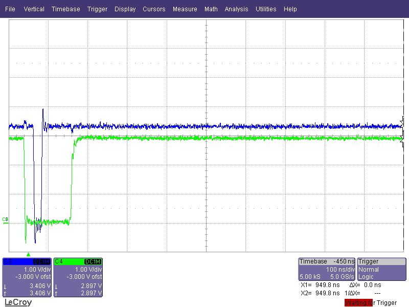
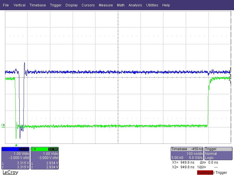
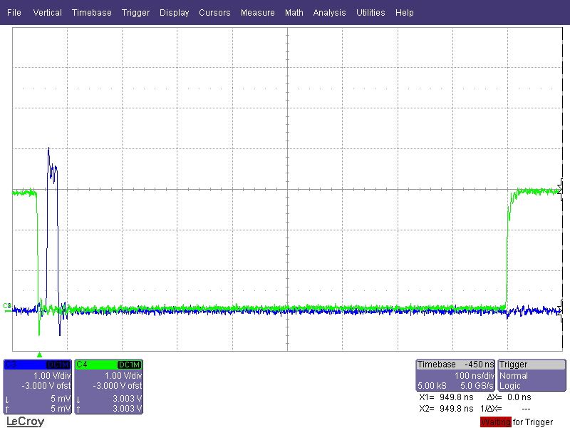
Normal Mode:
Chip select is green Chanel 4, RB1 is blue Chanel 3
This is with termination and you can see it times out
We tried inverting RB1 for a test of the status bit
- Mark as New
- Bookmark
- Subscribe
- Mute
- Subscribe to RSS Feed
- Permalink
- Report Inappropriate Content
Which RCW is used?
What are IFC CS1 settings?
- Mark as New
- Bookmark
- Subscribe
- Mute
- Subscribe to RSS Feed
- Permalink
- Report Inappropriate Content
CPU: Freescale LayerScape LS1021, Version: 2.0, (0x87001120)
Clock Configuration:
CPU0(ARMV7):1000 MHz,
Bus:300 MHz, DDR:800 MHz (1600 MT/s data rate),
Reset Configuration Word (RCW):
00000000: 0608000a 00000000 00000000 00000000
00000010: 20000000 00403900 e0025a00 21046000
00000020: 00000000 00000000 00000000 18000000
00000030: 00080000 481b7340 00000000 00000000
From file*******************************************************************
#define CONFIG_SYS_CPLD_BASE 0x7f000000
#define CPLD_BASE_PHYS CONFIG_SYS_CPLD_BASE
#define CONFIG_SYS_FPGA_CSPR_EXT (0x0)
#define CONFIG_SYS_FPGA_CSPR (CSPR_PHYS_ADDR(CPLD_BASE_PHYS) | \
CSPR_PORT_SIZE_16 | \
CSPR_MSEL_GPCM | \
CSPR_V)
#define CONFIG_SYS_FPGA_AMASK IFC_AMASK(16 * 1024 * 1024)
#define CONFIG_SYS_FPGA_CSOR (CSOR_GPCM_GPMODE_NORMAL | \
CSOR_GPCM_GPTO(256) | \
CSOR_GPCM_RGETA_EXT | \
CSOR_GPCM_WGETA_EXT | \
CSOR_GPCM_ADM_SHIFT(4) | \
CSOR_GPCM_BURST(2) | \
CSOR_GPCM_TRHZ_20 | \
CSOR_GPCM_BCTLD)
#define CONFIG_SYS_FPGA_FTIM0 (FTIM0_GPCM_TACSE(0x1) | \
FTIM0_GPCM_TEADC(0x01) | \
FTIM0_GPCM_TEAHC(0x01))
#define CONFIG_SYS_FPGA_FTIM1 (FTIM1_GPCM_TACO(0x01) | \
FTIM1_GPCM_TRAD(0x21))
#define CONFIG_SYS_FPGA_FTIM2 (FTIM2_GPCM_TCS(0x1) | \
FTIM2_GPCM_TCH(0x1) | \
FTIM2_GPCM_TWP(0x21))
#define CONFIG_SYS_FPGA_FTIM3 FTIM3_GPCM_TAAD(0x06)
From memory big endian******************************************************
IFC_CSPR1(0x153001c) = 0x7f000105
IFC_AMASK1(0x15300ac) = 0xff000000
IFC_CSOR1_GPCM(0x153013c) = 0x000c8201
IFC_FTIM0_CS1_GPCM(0x15301f0) = 0x10010001
IFC_FTIM1_CS1_GPCM(0x15301f4) = 0x01002100
IFC_FTIM2_CS1_GPCM(0x15301f8) = 0x01040021
IFC_FTIM3_CS1_GPCM(0x15301fc) = 0x18000000


