
- NXP Forums
- Product Forums
- General Purpose MicrocontrollersGeneral Purpose Microcontrollers
- i.MX Forumsi.MX Forums
- QorIQ Processing PlatformsQorIQ Processing Platforms
- Identification and SecurityIdentification and Security
- Power ManagementPower Management
- MCX Microcontrollers
- S32G
- S32K
- S32V
- MPC5xxx
- Other NXP Products
- Wireless Connectivity
- S12 / MagniV Microcontrollers
- Powertrain and Electrification Analog Drivers
- Sensors
- Vybrid Processors
- Digital Signal Controllers
- 8-bit Microcontrollers
- ColdFire/68K Microcontrollers and Processors
- PowerQUICC Processors
- OSBDM and TBDML
-
- Solution Forums
- Software Forums
- MCUXpresso Software and ToolsMCUXpresso Software and Tools
- CodeWarriorCodeWarrior
- MQX Software SolutionsMQX Software Solutions
- Model-Based Design Toolbox (MBDT)Model-Based Design Toolbox (MBDT)
- FreeMASTER
- eIQ Machine Learning Software
- Embedded Software and Tools Clinic
- S32 SDK
- S32 Design Studio
- Vigiles
- GUI Guider
- Zephyr Project
- Voice Technology
- Application Software Packs
- Secure Provisioning SDK (SPSDK)
- Processor Expert Software
-
- Topics
- Mobile Robotics - Drones and RoversMobile Robotics - Drones and Rovers
- NXP Training ContentNXP Training Content
- University ProgramsUniversity Programs
- Rapid IoT
- NXP Designs
- SafeAssure-Community
- OSS Security & Maintenance
- Using Our Community
-
-
- Home
- :
- General Purpose Microcontrollers
- :
- Kinetis Microcontrollers
- :
- MK10DN512 problem using pdb triggered adc with dma scatter/gather feature
MK10DN512 problem using pdb triggered adc with dma scatter/gather feature
- Subscribe to RSS Feed
- Mark Topic as New
- Mark Topic as Read
- Float this Topic for Current User
- Bookmark
- Subscribe
- Mute
- Printer Friendly Page
- Mark as New
- Bookmark
- Subscribe
- Mute
- Subscribe to RSS Feed
- Permalink
- Report Inappropriate Content
Hello!
I am triggering ADC0 via PDB. On conversion complete the ADC "triggers" the DMA channel, to write the conversion result to a RAM buffer. Since i have 3 inputs to the ADC and need 1024 samples per channel, i use the DMA scatter/gather feature to overload the TCD of the DMA channel with channel linking to perform another minor loop to update the ADCs SC1x register with the next input channel.
So far it seems to be working, but the order of entries in the SRAM buffer is not what I was hoping for. The first 510 entries are shifted into a new order (3-1-2), the next 510 entries order 2-3-1, the next 1-2-3 and so on..
I have attached my implementation, and would like to ask what I am doing wrong here, since I would love every entry in the order 1-2-3 as defined in the source array.
Thank you for your inputs,
pht
Original Attachment has been moved to: _dma.c.zip
Solved! Go to Solution.
- Mark as New
- Bookmark
- Subscribe
- Mute
- Subscribe to RSS Feed
- Permalink
- Report Inappropriate Content
Ok, I "fixed" the problem.
PDB is triggering the ADC. On conversion complete DMA updates the ADCs input channel in SC1A and in the ADC ISR the conversion result is being written to the SRAM buffer.
Sadly I wasnt able to get the system running without processor intervention, that is interrupts and reading/writing, for this application.
Have a nice day,
pht
- Mark as New
- Bookmark
- Subscribe
- Mute
- Subscribe to RSS Feed
- Permalink
- Report Inappropriate Content
Hi Philip,
I've had a brief look through the attachment, I hasn't found something wrong with the code.
I was wondering if you can clarify the order (3-1-2), order (2-3-1) and order (1-2-3).
I'm looking forward to your reply
Have a great day,
Ping
-----------------------------------------------------------------------------------------------------------------------
Note: If this post answers your question, please click the Correct Answer button. Thank you!
-----------------------------------------------------------------------------------------------------------------------
- Mark as New
- Bookmark
- Subscribe
- Mute
- Subscribe to RSS Feed
- Permalink
- Report Inappropriate Content
Hello Ping,
first of all, thank you for your answer!
By the correct order I mean the following: I have three input channels to the ADC. After a conversion DMA should change the ADCs input to the next one, alternating it in the order channel 1, channel 2, channel 3, back to channel 1, channel 2, channel 3, and so on. This is done in a minor loop updating the ADC SD1x register. Unfortunately, when doing minor loop linking, the maximal loop count is reduced to 9 bits. Since I need 3x10²⁰ samples from the ADC I update the DMA TCD 6 times (6x510 samples = 3x10²⁰ samples).
When I take a look in the buffer array, the order, in which the samples are being written into, is for the first 510 samples channel 3, channel 1, channel 2, instead of channel 1, channel 2, channel 3. After the first 510 entries in the buffer array the order switches to channel 2, channel 1, channel 3 and so on. After 1020 samples in the buffer array the order changes again to channel 1, channel 2, channel 3 and so on.
This causes a problem, because I would like the 3x10²⁰ entries all in the order channel 1, channel 2, channel 3, channel 1, channel 2, channel 3 and so on.
I hope I could clarify my question and I am looking forward to your reply.
Have a nice day,
pht
- Mark as New
- Bookmark
- Subscribe
- Mute
- Subscribe to RSS Feed
- Permalink
- Report Inappropriate Content
Hi Philip,
I think it can be the more easier to find out the root cause when simplify the DMA transmission.
So I 'd highly recommend you to check out the result when just start the DMA transmission without enable the DMA scatter/gather feature versus sample two ADC input channel with enable the enable the DMA scatter/gather feature.
Hope it helps and I'm looking forward to your updates.
Ping
- Mark as New
- Bookmark
- Subscribe
- Mute
- Subscribe to RSS Feed
- Permalink
- Report Inappropriate Content
Hi Ping,
i tried it with two input channels and scatter/gather enabled. What is happening is that the first entry in the ram buffer is actually the result from channel two. After the first 510 entries in the buffer, the order switches (eg 1-2-1-2..).
What i think is happening, is that the channel does not set back the source address correctly when a new TCD is loaded.
What are your thoughts about that?
Have a nice day,
pht
- Mark as New
- Bookmark
- Subscribe
- Mute
- Subscribe to RSS Feed
- Permalink
- Report Inappropriate Content
Hi Philip Tutzer,
Thanks for your reply.
I guess the first order is right, however the second writing order may overwrite the area that store the the first order writing.
In my opinion, the key point of the issue is to figure out the first order of the DMA write to RAM, so I modify the code to enable the end-of-major loop interrupt of the DMA channel 14 after first order of writing completes.
And in the ISR fuction, you can read the array area, then to check it out.
Modified code as below.
| //DMA 14 | ||
| DMA_CSR( 13 ) &= ~DMA_CSR_DONE_MASK; | ||
| DMA_SADDR( 14 ) = DMA_SADDR_SADDR( (uint32_t)&sram_adc_conf[ 0 ] ); | // 8 bits from adc0_channel | |
| DMA_SOFF( 14 ) = DMA_SOFF_SOFF( 1 ); | // offset = 1 byte | |
| DMA_SLAST( 14 ) = DMA_SLAST_SLAST( 0 ); | // set back 3 bytes after major loop | |
| DMA_DADDR( 14 ) = DMA_DADDR_DADDR( (uint32_t)&ADC0_SC1A ); | // destination address is ADC0 status and control register | |
| DMA_DOFF( 14 ) = DMA_DOFF_DOFF( 0 ); | // no offset for destination | |
| DMA_DLAST_SGA( 14 ) = DMA_DLAST_SGA_DLASTSGA( 0 ); | // no set back | |
| DMA_NBYTES_MLNO( 14 ) = DMA_NBYTES_MLNO_NBYTES( 1 ); | // minor byte transfer count = 1 byte | |
| DMA_BITER_ELINKNO( 14 ) = 0 | ||
| | 0x01; | // 1 readings | |
| DMA_CITER_ELINKNO( 14 ) = 0 | ||
| | 0x01; | // 1 readings | |
| DMA_ATTR( 14 ) = 0 | ||
| | DMA_ATTR_SSIZE( DMA_SIZE_8BIT ) | // 8 bit data size | |
| | DMA_ATTR_DSIZE( DMA_SIZE_8BIT ); | ||
| DMA_CSR( 14 ) |= DMA_CSR_INTMAJOR_MASK; | // The end-of-major loop interrupt is enabled |
Have a great day,
Ping
-----------------------------------------------------------------------------------------------------------------------
Note: If this post answers your question, please click the Correct Answer button. Thank you!
-----------------------------------------------------------------------------------------------------------------------
- Mark as New
- Bookmark
- Subscribe
- Mute
- Subscribe to RSS Feed
- Permalink
- Report Inappropriate Content
Hello!
I did take a look into the registers with IRQ set on DMA channel 14 and could not find something interesting/wrong.
I guess the first entry in the buffer array is generated because the ADC is configured with an input channel,
ADC0_SC1A = sram_adc_conf[ 0 ]; // line 303
before DMA is able to set it to the first "correct" channel, eg. PDB triggers ADC, ADC is set with channel 3, DMA takes the result after CoCo and then updates the ADC input channel with the first channel from its input array (line 58):
static char sram_adc_conf[3] = { CH1, // temp sensor
CH2, // bandgap
CH3 }; // V_refsh
Not perfect, but manageable.
The main problem arrises when the following TCDs are loaded, because the entries still begin with channel 3 though they should start with channel 1. The only thing I can think of is, that DMA does not set back the source address after the major loop finishes. This means, that I have double entries in the buffer array on every TCD transition, which messes up the results, beause I cant guarantee the correct sampling rate for the corresponding input channels.
The DMA channel 14 handles the updating of the ADC input channels:
//DMA 14
DMA_CSR( 14 ) &= ~DMA_CSR_DONE_MASK;
DMA_SADDR( 14 ) = DMA_SADDR_SADDR( (uint32_t)&sram_adc_conf[ 0 ] ); // 8 bits from adc0_channel
DMA_SOFF( 14 ) = DMA_SOFF_SOFF( 1 ); // offset = 1 byte
DMA_SLAST( 14 ) = DMA_SLAST_SLAST( -3 ); // set back 3 bytes after major loop
DMA_DADDR( 14 ) = DMA_DADDR_DADDR( &ADC0_SC1A ); // destination address is ADC0 status and control register
DMA_DOFF( 14 ) = DMA_DOFF_DOFF( 0 ); // no offset for destination
DMA_DLAST_SGA( 14 ) = DMA_DLAST_SGA_DLASTSGA( 0 ); // no set back
DMA_NBYTES_MLNO( 14 ) = DMA_NBYTES_MLNO_NBYTES( 1 ); // minor byte transfer count = 1 byte
DMA_BITER_ELINKNO( 14 ) = 0
| 0x03; // 3 readings
DMA_CITER_ELINKNO( 14 ) = 0
| 0x03; // 3 readings
DMA_ATTR( 14 ) = 0
| DMA_ATTR_SSIZE( DMA_SIZE_8BIT ) // 8 bit data size
| DMA_ATTR_DSIZE( DMA_SIZE_8BIT );
DMA_CSR( 14 ) = 0; // no IRQ enable, no linking after major loop
DMA 15s TCD is being overloaded with new TCDs as soon as the max value for iterations is reached:
tcd[ 0 ].CSR &= ~DMA_CSR_DONE_MASK;
tcd[ 0 ].SADDR = (uint32_t)&ADC0_RA; // source address, ADC0 result register
tcd[ 0 ].DADDR = (uint32_t)&adc_result_buffer[ 0 ]; // destination address in SRAM
tcd[ 0 ].SOFF = 0x00;
tcd[ 0 ].DOFF = 0x02;
tcd[ 0 ].ATTR = 0
| DMA_ATTR_SSIZE( DMA_SIZE_16BIT )
| DMA_ATTR_DSIZE( DMA_SIZE_16BIT );
tcd[ 0 ].NBYTES_MLNO = 0x02;
tcd[ 0 ].CITER_ELINKYES = 0
| DMA_CITER_ELINKYES_ELINK_MASK // enable channel-to-channel linking on minor-loop complete
| DMA_CITER_ELINKYES_CITER( AD_BUFFER_LEN ) // current major loop count
| DMA_CITER_ELINKYES_LINKCH( 14 );
tcd[ 0 ].SLAST = 0;
tcd[ 0 ].DLASTSGA = (uint32_t)&tcd[ 1 ]; // to next TCD
tcd[ 0 ].CSR = DMA_CSR_ESG_MASK;
tcd[ 0 ].BITER_ELINKYES = 0
| DMA_BITER_ELINKYES_BITER( AD_BUFFER_LEN ) // 511 samples
| DMA_BITER_ELINKYES_ELINK_MASK // enable channel to channel linking
| DMA_BITER_ELINKYES_LINKCH( 14 ); // link to channel 14
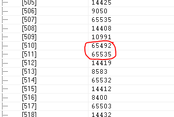
AD_BUFFER_LEN is 511, the next DADDR (of tcd[ 1 ]) is 511 to compensate for the wrong entry in pos 1, and so on. The entry should be the result of the conversion of CH1 (temp sensor) but actually is the result of the conversion of the reference voltage.
I attached a screenshot of the results in the array at position 510 in the array, but it is the same at position 1022, 1533, 2044, 2555.
Have a nice day,
pht
- Mark as New
- Bookmark
- Subscribe
- Mute
- Subscribe to RSS Feed
- Permalink
- Report Inappropriate Content
Hi Philip Tutzer,
Thanks for your reply.
I also agree with your explanation.
However I still have one query, what's the exactly time do you check out the vaue of the array of the adc_result_buffer[RAM_BUF_LEN].
I'm looking forward your clarification.
Have a great day,
Ping
-----------------------------------------------------------------------------------------------------------------------
Note: If this post answers your question, please click the Correct Answer button. Thank you!
-----------------------------------------------------------------------------------------------------------------------
- Mark as New
- Bookmark
- Subscribe
- Mute
- Subscribe to RSS Feed
- Permalink
- Report Inappropriate Content
Hi!
I just set a few breakpoints to asm("nop") instructions.
However, I changed the code, so that PDB is directly triggering DMA15, which then sets the ADC SC1A register. The ADC is set to software trigger mode. DMA14 should then read the value of ADC´s RA register as soon as the CoCo bit is set.
So far DMA15 seems to do its job and I can the the SC1A register updated properly, but the ADC does not start the conversion. I set the ADC interrupt, but it is never triggered, because the ADC does not finish any conversion.
Do you see an error in this application?
//---PDB--------------------------------------------------------------------------------------------
#define PDB_MOD_VALUE 32000 // counter running at 48MHz = 667us -> 1.5kHz
#define PDB_DLY_VALUE ( PDB_MOD_VALUE )
// pdb runs off BUS clock frequency
void config_pdb( void )
{
SIM_SCGC6 |= SIM_SCGC6_PDB_MASK ; // enable PDB clock
PDB0_SC = 0
| PDB_SC_LDMOD( 0 ) // registers updated when PDB counter reaches MOD or trigger event
| PDB_SC_PRESCALER( 0 ) // highest speed
| PDB_SC_TRGSEL( 15 ) // select software trigger
| PDB_SC_PDBEN_MASK // enable the PDB
| PDB_SC_MULT( 0 ) // highest speed
| PDB_SC_CONT_MASK // continuous mode
| PDB_SC_DMAEN_MASK;
PDB0_MOD = PDB_MOD_MOD( PDB_MOD_VALUE ); // counter resets at this value
PDB0_CH0C1 = 0
| PDB_C1_EN( 0 ) // channel 0, pre-trigger/trigger 0 enable (ADC0)
| PDB_C1_TOS( 0 ); // channel 0, pre_trigger/trigger 0 delayed (not bypassed)
PDB0_CH0DLY0 = PDB_DLY_DLY( PDB_DLY_VALUE ); // delay = 666uS
PDB0_SC |= PDB_SC_LDOK_MASK; // load registers with written values
}
void pdb_trigger( void )
{
PDB0_SC |= PDB_SC_SWTRIG_MASK; // software trigger
}
//----DMA-------------------------------------------------------------------------------------------
#define DMA_SIZE_8BIT 0
#define DMA_SIZE_16BIT 1
#define AD_LOOP_LEN 1
#define RAM_BUF_LEN 511
#define CH1 0x5A // 26
#define CH2 0x5B // 27
#define CH3 0x5D // 29
static volatile uint16_t adc_result_buffer[ RAM_BUF_LEN ] = { 0 }; // SRAM buffer
static const uint8_t sram_adc_conf[3] = { CH1,
CH2,
CH3 };
void configDMA( void )
{
SIM_SCGC7 |= SIM_SCGC7_DMA_MASK; // enable DMA clock
SIM_SCGC6 |= SIM_SCGC6_DMAMUX_MASK ; // enable DMAMUX clocking
// DMA channel 15 --> selects ADC input channel
DMA_CSR( 15 ) &= ~DMA_CSR_DONE_MASK;
DMA_SADDR( 15 ) = DMA_SADDR_SADDR( (uint32_t)&sram_adc_conf[ 0 ] );
DMA_DADDR( 15 ) = DMA_DADDR_DADDR( &ADC0_SC1A );
DMA_SOFF( 15 ) = 0x01;
DMA_DOFF( 15 ) = 0x00;
DMA_ATTR( 15 ) = 0
| DMA_ATTR_SSIZE( DMA_SIZE_8BIT )
| DMA_ATTR_DSIZE( DMA_SIZE_8BIT );
DMA_NBYTES_MLNO( 15 ) = 0x01;
DMA_CITER_ELINKNO( 15 ) = 0
| 0x03; // 3 channels
DMA_SLAST( 15 ) = DMA_SLAST_SLAST( -3 );
DMA_DLAST_SGA( 15 ) = 0;
DMA_CSR( 15 ) = 0;
DMA_BITER_ELINKNO( 15 ) = 0
| 0x03;
// DMA channel 14 --> gets triggered by CoCo of ADC and writes result to array
DMA_CSR( 14 ) &= ~DMA_CSR_DONE_MASK;
DMA_SADDR( 14 ) = (uint32_t)&ADC0_RA;
DMA_DADDR( 14 ) = DMA_DADDR_DADDR( &adc_result_buffer[ 0 ] );
DMA_SOFF( 14 ) = 0x00;
DMA_DOFF( 14 ) = 0x02;
DMA_ATTR( 14 ) = 0
| DMA_ATTR_SSIZE( DMA_SIZE_16BIT )
| DMA_ATTR_DSIZE( DMA_SIZE_16BIT );
DMA_NBYTES_MLNO( 14 ) = 0x02;
DMA_CITER_ELINKNO( 14 ) = 0
| 0x01;
DMA_SLAST( 14 ) = 0;
DMA_DLAST_SGA( 14 ) = 0;
DMA_CSR( 14 ) = 0;
DMA_BITER_ELINKNO( 14 ) = 0
| 0x01;
DMAMUX_CHCFG15 = DMAMUX_CHCFG14 = 0;
DMAMUX_CHCFG15 = 0
| DMAMUX_CHCFG_ENBL_MASK // enable DMA channel
| DMAMUX_CHCFG_SOURCE( 58 ); // PDB
DMAMUX_CHCFG14 = 0
| DMAMUX_CHCFG_ENBL_MASK // enable DMA channel
| DMAMUX_CHCFG_SOURCE( 40 ); // ADC0
DMA_ERQ = 0
| DMA_ERQ_ERQ15_MASK // enable DMA on hardware service request
| DMA_ERQ_ERQ14_MASK;
}
//----ADC-------------------------------------------------------------------------------------------------------------------------------
void config_adc( void )
{
ADC1_SC1A = 0
| 0x1F; // ADC1 module disabled
SIM_SCGC6 |= SIM_SCGC6_ADC0_MASK; // enable ADC0 clock
ADC0_CFG1 = 0
| ADC_CFG1_ADIV( 3 ) // CLK / 8 = 96MHz / 8 = 12MHz
| ADC_CFG1_ADLSMP_MASK // long sample time
| ADC_CFG1_MODE( 3 ) // 16bit conversion
| ADC_CFG1_ADICLK( 3 ), // Asynchronous clock
ADC0_CFG2 = 0
| ADC_CFG2_ADLSTS( 0 ); // default longest sample time
ADC0_SC2 = 0
| ADC_SC2_REFSEL( 0 ) // default voltage reference
| ADC_SC2_DMAEN_MASK; // DMA enabled
ADC0_SC2 &= ~ADC_SC2_ADTRG_MASK;
ADC0_SC3 = 0;
}
//----Init()-------------------------------------------------------------------------------------------------------------------------------
int ADC_DMA_PDB_init( void )
{
config_adc();
configDMA();
config_pdb();
pdb_trigger();
return 0;
}
Have a nice day,
pht
- Mark as New
- Bookmark
- Subscribe
- Mute
- Subscribe to RSS Feed
- Permalink
- Report Inappropriate Content
Hi Philip Tutzer,
I think of the new scenario can eliminate the double sampling error, and after had a brief look through the code above, I hasn't found any errors except that the period of the PDB interrup delay may take the shorter timer than the ADC sampling time, in another word, the ADC would start to sample the input channle after the DMA channel 15 update the ADC SC1A register.
And I also like to suggest that you enable the PDB Interrupt, then update the the ADC SC1A register in the PDB's interrupt function.
Have a great day,
Ping
-----------------------------------------------------------------------------------------------------------------------
Note: If this post answers your question, please click the Correct Answer button. Thank you!
-----------------------------------------------------------------------------------------------------------------------
- Mark as New
- Bookmark
- Subscribe
- Mute
- Subscribe to RSS Feed
- Permalink
- Report Inappropriate Content
Ok, I "fixed" the problem.
PDB is triggering the ADC. On conversion complete DMA updates the ADCs input channel in SC1A and in the ADC ISR the conversion result is being written to the SRAM buffer.
Sadly I wasnt able to get the system running without processor intervention, that is interrupts and reading/writing, for this application.
Have a nice day,
pht
- Mark as New
- Bookmark
- Subscribe
- Mute
- Subscribe to RSS Feed
- Permalink
- Report Inappropriate Content
Ok, I think I know whats happening:
After the last major loop, which would be number 510 in my application, the last ADC input channel is channel 3 from the input array. When the next TCD is loaded, DMA doesnt update ADCs SC1A, but waits for the CoCo signal from the ADC. So the ADC gets triggered again by PDB, the old input channel (channel 3) is still stored in SC1A, and there we have the double entries on TCD transition.
I guess there is no possibility in sampling 3 alternating channels with 1024 samples per channel, writing the results into a 2*1024 array into SRAM, at least not with PDB triggered ADC and DMA scatter/gather enabled.
pht