- NXP Forums
- Product Forums
- General Purpose MicrocontrollersGeneral Purpose Microcontrollers
- i.MX Forumsi.MX Forums
- QorIQ Processing PlatformsQorIQ Processing Platforms
- Identification and SecurityIdentification and Security
- Power ManagementPower Management
- MCX Microcontrollers
- S32G
- S32K
- S32V
- MPC5xxx
- Other NXP Products
- Wireless Connectivity
- S12 / MagniV Microcontrollers
- Powertrain and Electrification Analog Drivers
- Sensors
- Vybrid Processors
- Digital Signal Controllers
- 8-bit Microcontrollers
- ColdFire/68K Microcontrollers and Processors
- PowerQUICC Processors
- OSBDM and TBDML
-
- Solution Forums
- Software Forums
- MCUXpresso Software and ToolsMCUXpresso Software and Tools
- CodeWarriorCodeWarrior
- MQX Software SolutionsMQX Software Solutions
- Model-Based Design Toolbox (MBDT)Model-Based Design Toolbox (MBDT)
- FreeMASTER
- eIQ Machine Learning Software
- Embedded Software and Tools Clinic
- S32 SDK
- S32 Design Studio
- Vigiles
- GUI Guider
- Zephyr Project
- Voice Technology
- Application Software Packs
- Secure Provisioning SDK (SPSDK)
- Processor Expert Software
-
- Topics
- Mobile Robotics - Drones and RoversMobile Robotics - Drones and Rovers
- NXP Training ContentNXP Training Content
- University ProgramsUniversity Programs
- Rapid IoT
- NXP Designs
- SafeAssure-Community
- OSS Security & Maintenance
- Using Our Community
-
-
- Home
- :
- General Purpose Microcontrollers
- :
- Kinetis Microcontrollers
- :
- Measuring clock in KEA-128
Measuring clock in KEA-128
- Subscribe to RSS Feed
- Mark Topic as New
- Mark Topic as Read
- Float this Topic for Current User
- Bookmark
- Subscribe
- Mute
- Printer Friendly Page
Measuring clock in KEA-128
- Mark as New
- Bookmark
- Subscribe
- Mute
- Subscribe to RSS Feed
- Permalink
- Report Inappropriate Content
Hi,
I want to measure my clock in KEA-128.I am doing this by toggling a GPIO pin in it.I am running my clock at 20Mhz which was the standard example given by NXP(Freescale).But my scope is reading only 583 Khz only.I think I am missing something in it.
I want to know the bus clock per instruction in KEA-128?
The clock per instruction of peripherals?
Can you suggest me a good method to measure the Clock of KEA-128 other than toggling a GPIO?
- Mark as New
- Bookmark
- Subscribe
- Mute
- Subscribe to RSS Feed
- Permalink
- Report Inappropriate Content
Hello Vignest,
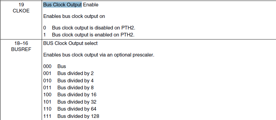
You can check the bus clock on the pin of PTH2 .
First enable the "bus clock output " of this register :
SIM_SOPT0 -> CLKOE
Hope it helps !
Have a great day,
Alice Yang
-----------------------------------------------------------------------------------------------------------------------
Note: If this post answers your question, please click the Correct Answer button. Thank you!
-----------------------------------------------------------------------------------------------------------------------
- Mark as New
- Bookmark
- Subscribe
- Mute
- Subscribe to RSS Feed
- Permalink
- Report Inappropriate Content
Hi Alice and David,
Both of your answers are working for me.I want to know why normal GPIO toggling won't work.Is it because of number of instructions taken to do it?
Can you please provide any diagram or place where it is mentioned that PTH2 is directly connected to the system clock.Thank you ffor your help.
- Mark as New
- Bookmark
- Subscribe
- Mute
- Subscribe to RSS Feed
- Permalink
- Report Inappropriate Content
Hi VIGNESH BALAJI,
See you again!
Actually, about this question, I already answer you in your CASE:
GPIO toggle is using the GPIO module, the GPIO module speed is not as faster as the bus clock.
Besides, if you use the GPIO, it still related to the instuction cycles, the compilier, the optimization function,ect.
All these factors will affect the GPIO toggle speed, you can check the according asm code, you will find the detals. If you still want to use GPIO, you can choose FGPIO, it will faster than the GPIO. Write the code, don't use the while, because while still need a lot of cycles, you can use the FGPIO code one by one directly.
eg.
FGPIOE_PRTOR=0X02;
FGPIOE_PRTOR=0X02;
FGPIOE_PRTOR=0X02;
FGPIOE_PRTOR=0X02;
FGPIOE_PRTOR=0X02;
...
But I suggest you use the method which I told you to test the bus clock:
Configure SIM_SOPT0[CLKOE]=1, SIM_SOPT0[BUSFREF]=0, Bus clock output is enabled on PTH2.
This will output bus clock directly!
Wish it helps you!
Have a great day,
Jingjing
-----------------------------------------------------------------------------------------------------------------------
Note: If this post answers your question, please click the Correct Answer button. Thank you!
-----------------------------------------------------------------------------------------------------------------------
- Mark as New
- Bookmark
- Subscribe
- Mute
- Subscribe to RSS Feed
- Permalink
- Report Inappropriate Content
Thank you jing,
The FTM method was good
- Mark as New
- Bookmark
- Subscribe
- Mute
- Subscribe to RSS Feed
- Permalink
- Report Inappropriate Content
OK, that's very good!
If you still have any question, please let me know!
Have a great day,
Jingjing
-----------------------------------------------------------------------------------------------------------------------
Note: If this post answers your question, please click the Correct Answer button. Thank you!
-----------------------------------------------------------------------------------------------------------------------
- Mark as New
- Bookmark
- Subscribe
- Mute
- Subscribe to RSS Feed
- Permalink
- Report Inappropriate Content
Hi Jing,
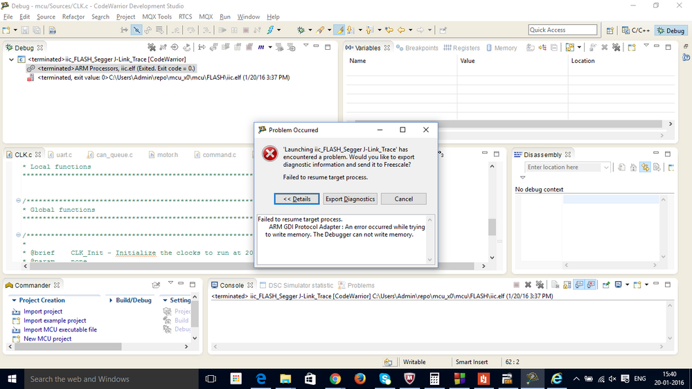
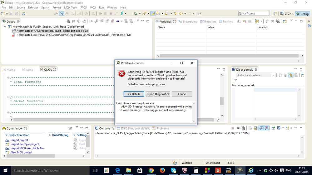
I am having a problem now.I ran my bus clock at 48 Mhz using the below code change.Now I am not able to flash my code.Can you tell me what went wrong and how to fix it?
SIM_SOPT0 = SIM_SOPT0_CLKOE_MASK;
void Clk_Init()
{
ICS_C1|=ICS_C1_IRCLKEN_MASK; /* Enable the internal reference clock*/
while(!(ICS_S & ICS_S_LOCK_MASK)); /* Wait for PLL lock, now running at 40 MHz (1280 * 31.25Khz) */
ICS_S |= ICS_S_LOCK_MASK ; /* Clear Loss of lock sticky bit */
}
This was the error message I got.I am using segger to Flash the code.
- Mark as New
- Bookmark
- Subscribe
- Mute
- Subscribe to RSS Feed
- Permalink
- Report Inappropriate Content
Hi VIGNESH BALAJI,
Now please follow me to mass erase your TRK-KEA128 at first, besides, you can't use this code:SIM_SOPT0 = SIM_SOPT0_CLKOE_MASK;, this code is not correct.
Mass erase the TRK-KEA128 process:
1. install the JLINK driver
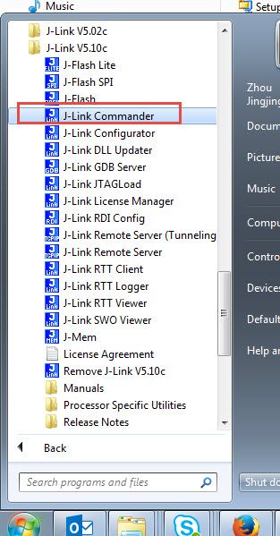
After you install the JLINK driver, you will find the J-Link Commander software.
2. Make sure you are using the JLINK firmware in your TRK-KEA128, from the picture which you give me, I find you already using the JLINK firmware.
The following step is very important!
3, unplug the TRK-KEA128 USB cable in J16, hold on the SW3, don't release the SW3 then plug the USB cable to your PC.
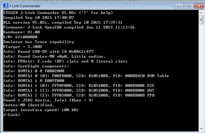
4,don't release the SW3, open J-LINK Commander windows:
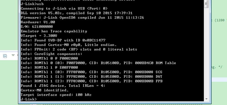
You can find the JLINK can find the core now!
5.don't release the SW3, input command in the JLINK Commander windows: unlock kinetis
Waiting the : Timeout while unlocking device come out
6, release the SW3, input command in the JLINK Commander windows: usb
Until now, your chip is masserased, you can program it again, but take care,modify your code:
SIM_SOPT0 = SIM_SOPT0_CLKOE_MASK;
to
SIM_SOPT0 |= SIM_SOPT0_CLKOE_MASK;
Because if you use the SIM_SOPT0 =, you will clear bit SWDE, this will disable the SWD debug interface, that's why you can't program agan!
Please follow my step, mass erase your chip at first!
Wish it helps you!
Have a great day,
Jingjing
-----------------------------------------------------------------------------------------------------------------------
Note: If this post answers your question, please click the Correct Answer button. Thank you!
-----------------------------------------------------------------------------------------------------------------------
- Mark as New
- Bookmark
- Subscribe
- Mute
- Subscribe to RSS Feed
- Permalink
- Report Inappropriate Content
Hi Jing,
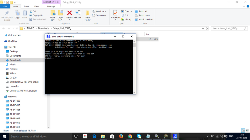
I am actually getting this message.I explicitly grounded the reset pin for the holding switch instruction.
I am actually using J-Link STR9 Commander.Is that Fine???
- Mark as New
- Bookmark
- Subscribe
- Mute
- Subscribe to RSS Feed
- Permalink
- Report Inappropriate Content
Hi Jing,
It is not detecting KEA-128.I went sent that in settings also both by selecting ARM-M0+ and by Manufactureres list(where I selected as SKEAZ-1284 and tried both security and normal one).
Please combine all the 3 replies from me.
- Mark as New
- Bookmark
- Subscribe
- Mute
- Subscribe to RSS Feed
- Permalink
- Report Inappropriate Content
Hi VIGNESH BALAJI,
I know if you just connect the board, then use the JLINK COMANDER you will can't find the core, but did you follow my step?
Hold on the SW3 before you plug the USB cable, and don't release it, just hold on it all the time before you do the mass erase!
I already use your code, and use my method do the mass erase a lot of times, each time I can successfully mass erase it, and after you mass erase the chip, you can release the SW3.
Take care, hold on the SW3 before your board is power on, and keep on holding it after you power on and before you successfully mass erased it.
Wish it helps you!
Jingjing
-----------------------------------------------------------------------------------------------------------------------
Note: If this post answers your question, please click the Correct Answer button. Thank you!
-----------------------------------------------------------------------------------------------------------------------
- Mark as New
- Bookmark
- Subscribe
- Mute
- Subscribe to RSS Feed
- Permalink
- Report Inappropriate Content
Hi VIGNESH BALAJI,
I have not used J-LINK STR9 Commander before, I am not sure whether it works on the kinetis.
I suggest you install the JLINK driver which I suggest before, then you will find the JLINK COMMANDER
Wish it helps you!
Jingjing
-----------------------------------------------------------------------------------------------------------------------
Note: If this post answers your question, please click the Correct Answer button. Thank you!
-----------------------------------------------------------------------------------------------------------------------
- Mark as New
- Bookmark
- Subscribe
- Mute
- Subscribe to RSS Feed
- Permalink
- Report Inappropriate Content
Hi Jing,
I checked the voltage at the SWD pin.It is not pulled high.It is at 2 volts.If the SWD is disabled will the reset pin also be disturbed ? I will try by Explicitly pulling it low and then high.
- Mark as New
- Bookmark
- Subscribe
- Mute
- Subscribe to RSS Feed
- Permalink
- Report Inappropriate Content
Hi VIGNGSH BALAJI,
Please follow my method to mass erase your chip at first, otherwise, you can't program it, because the chip's SWD pin function has been disabled by your code.
Wish it helps you!
Have a great day,
Jingjing
-----------------------------------------------------------------------------------------------------------------------
Note: If this post answers your question, please click the Correct Answer button. Thank you!
-----------------------------------------------------------------------------------------------------------------------
- Mark as New
- Bookmark
- Subscribe
- Mute
- Subscribe to RSS Feed
- Permalink
- Report Inappropriate Content
Hi Jing,
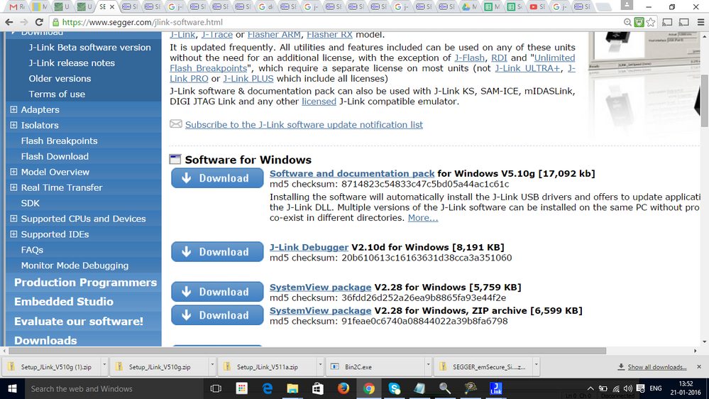
In the J-link Driver Link you gave me.I downloaded the Software and Documentation pack.In that I found only J-link STR commander under version 5.10.
Your version shows 5.02 .Should I go back to the older version If so where Can I find them I am trying Hard to Find them.Can you please chaeck out whether the package I downloaded is right?
I have attached the Screenshot of what I downloaded
- Mark as New
- Bookmark
- Subscribe
- Mute
- Subscribe to RSS Feed
- Permalink
- Report Inappropriate Content
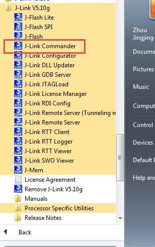
See my V5.10g install information:
I still can see the JLINK Commander tool!
Jingjing
- Mark as New
- Bookmark
- Subscribe
- Mute
- Subscribe to RSS Feed
- Permalink
- Report Inappropriate Content
My version is 5.10c, not 5.02, you see the wrong item.
I will try version 5.10g, please wait a moment!
Jingjing
- Mark as New
- Bookmark
- Subscribe
- Mute
- Subscribe to RSS Feed
- Permalink
- Report Inappropriate Content
Hello VIGNESH,
- How about your code to toggling the GPIO pin ?
- About the bus clock output , please refer to the KEA128RM, the PTH2 pin is the bus clock pin,
and configure the "CLOKOE" and "BUSREF" to select the value of the pth2 pin out put.
Hope it helps
Have a great day,
Alice Yang
-----------------------------------------------------------------------------------------------------------------------
Note: If this post answers your question, please click the Correct Answer button. Thank you!
-----------------------------------------------------------------------------------------------------------------------
- Mark as New
- Bookmark
- Subscribe
- Mute
- Subscribe to RSS Feed
- Permalink
- Report Inappropriate Content
I would suggest using the FlexTimer in PWM mode, and have it toggle one of the outputs. It uses bus clock as the clock source and is much more straightforward than disassembling the source and computing instruction cycles. Not all instructions use the same number of clock cycles.
- Mark as New
- Bookmark
- Subscribe
- Mute
- Subscribe to RSS Feed
- Permalink
- Report Inappropriate Content
Hi,
Is there a constrain that we should not run the bus clock at 48Mhz???
I modified my clock like this and found that my controller is not in a flashable state.
Can you tell me what has happened behind this?I am not able to flash my controller after this?
This was my clock code
SIM_SOPT0 = SIM_SOPT0_CLKOE_MASK;
void Clk_Init()
{
ICS_C1|=ICS_C1_IRCLKEN_MASK; /* Enable the internal reference clock*/
while(!(ICS_S & ICS_S_LOCK_MASK));
ICS_S |= ICS_S_LOCK_MASK ; /* Clear Loss of lock sticky bit */
}
- Mark as New
- Bookmark
- Subscribe
- Mute
- Subscribe to RSS Feed
- Permalink
- Report Inappropriate Content
The bus clock cannot run faster than 24MHz. You will have to change the SIM_CLKDIV register to make sure the bus clock is divided by 2 from the core clock BEFORE you set the ICS for 48MHz.

